
 My Inquiry
 My Account


Analog Devices Inc./Maxim Integrated DS2182QN
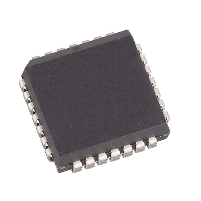
- Part No.:
- DS2182QN
- Manufacturer:
- Analog Devices Inc./Maxim Integrated
- Category:
- Specialized
- Package:
- 28-LCC (J-Lead)
- Datasheet:
-
 DS2182QN.pdf
- Description:
- IC MONITOR LINE T1 IND 28-PLCC
- Quantity:
- Payment:

- Shipping:

Inventory:443
Please send an inquiry. Send us your inquiry, and we will respond immediately.
Product details
Overview
DS2182QN from Maxim Integrated is a T1 line monitor IC designed for real-time performance monitoring of T1 digital telecommunication lines. It performs framing synchronization (Superframe and Extended Superframe), counts four distinct error types (16-bit bipolar violation, 8-bit CRC, 8-bit OOF, 8-bit frame bit error), and delivers alarm outputs including RLOS, RYEL, RBV, and RFER. It operates at -40°C to +85°C in 28-pin PLCC packaging and supports 1.544MHz receive clock input.
For engineers reviewing the DS2182QN datasheet, DS2182QN pinout, DS2182QN application, or DS2182QN equivalent, key selection considerations include its dual-framing mode support (193S/193E), on-chip burst-mode serial interface for fast status polling, auto-counter reset capability, B8ZS codeword detection, and carrier loss detection via 192-zero-string monitoring.
Technical Context
The DS2182QN implements a hardware-based receive synchronizer that detects loss-of-frame/multiframe alignment and performs off-line resync using configurable criteria (RCR1.3/RCR1.2). It supports two framing modes-12-frame Superframe (193S) and 24-frame Extended Superframe (193E)-with independent sync algorithms, CRC6 validation, and S-bit/FDL-based yellow alarm detection.
Its serial port uses an 8-bit address/command byte (ACB) with LSB-first data transfer, burst-mode capability (ACB.7), and asynchronous operation relative to RCLK. All four error counters are presettable, saturate at defined thresholds (65,535 for BVCR, 255 for others), and generate latched status bits (RSR1/RSR2) with maskable interrupts via RIMR1/RIMR2.
Key Specifications
| Parameter | Value and Actual Design Meaning |
|---|---|
| Supply Voltage | 5.0V single supply; enables direct compatibility with legacy TTL/CMOS logic without level-shifting. |
| Data Rate Support | 1.544MHz T1 line rate; precisely matches North American T1 standard timing requirements. |
| Framing Modes | Supports both 193S (Superframe) and 193E (Extended Superframe); selected via RCR2.4 bit. |
| Error Counters | Four dedicated hardware counters: 16-bit BVCR (bipolar violations), three 8-bit registers (CRC, OOF, frame bit errors). |
| Alarm Outputs | Dedicated open-drain or push-pull outputs: RLOS (loss-of-sync), RYEL (yellow alarm), RBV (bipolar violation), RFER (frame error). |
| Serial Interface | 4-wire SPI-compatible port (SDI/SDO/SCLK/CS); supports burst read/write for rapid status acquisition across 11 registers. |
| Operating Temperature | -40°C to +85°C; qualified for industrial-grade telecom infrastructure deployment. |
| Package | 28-pin PLCC (Plastic Leaded Chip Carrier); surface-mount compatible with automated assembly and thermal reliability for telecom chassis. |
Pinout & Package
DS2182QN is housed in a 28-pin PLCC package with gull-wing leads, optimized for thermal dissipation and board-level reliability in telecom line cards. Pin numbering follows standard PLCC top-view convention (pin 1 at index corner).
| Pin/Terminal | Circuit Role | Design Meaning |
|---|---|---|
| INT | Interrupt Output | Active-low open-drain alarm interrupt signaling latched status changes in RSR1/RSR2; requires external pull-up. |
| SDI / SDO / SCLK / CS | Serial Port Interface | Full-duplex SPI-like control interface; enables configuration, status readback, and counter polling without disrupting T1 monitoring. |
| RPOS / RNEG | Bipolar Data Inputs | Differential NRZ data inputs sampled on RCLK falling edge; internally terminated for T1 line impedance matching. |
| RCLK | Receive Clock Input | 1.544MHz primary clock derived from incoming T1 signal; drives all internal timing and sampling functions. |
| RFSYNC / RMSYNC | Frame/Multiframe Sync Outputs | 8kHz frame sync (RFSYNC) and multiframe sync (RMSYNC) outputs used for downstream timing alignment and channel extraction. |
| RSER / RLINK / RABCD | Data Extraction Outputs | RSER = raw serial data; RLINK = FDL/S-bit data; RABCD = ABCD signaling bits - all synchronized to RCLK for deterministic demuxing. |
| RLOS / RYEL / RBV / RFER | Alarm Status Outputs | Dedicated real-time alarm indicators enabling immediate system response without software polling overhead. |
| VDD / VSS / TEST | Power & Test | VDD = 5V supply; VSS = signal ground; TEST = tied to VSS for normal operation; no test mode activation required. |
Key Features
| Feature | Design Value |
|---|---|
| Burst-Mode Serial Access | Enables full 11-register read/write in one transaction, reducing host CPU overhead during status polling and initialization. |
| Auto Counter Reset | When enabled (RCR1.4), reading any counter register automatically clears all four error counters-eliminating race conditions during status capture. |
| Dual Framing Mode Flexibility | Hardware-selectable 193S or 193E operation via RCR2.4 allows field-deployable adaptation to legacy or modern T1 network configurations. |
| Configurable Resync Algorithm | Adjustable sync validation depth (10 vs. 24 framing bits) and CRC6 confirmation (RCR1.2/RCR1.3) balances false-framing immunity against reframe latency. |
| Comprehensive Alarm Detection | Detects and flags yellow/blue alarms, carrier loss (192 zeros), bipolar violations, OOF, frame errors, and B8ZS codewords-covering all ANSI T1.231 compliance requirements. |
| Asynchronous Serial Operation | Serial port operates independently of RCLK, allowing host access at any time without disrupting real-time line monitoring or introducing timing jitter. |
Applications
| Channel Bank Monitoring | T1 Line Card Diagnostics |
|---|---|
Use Scenario: Real-time health monitoring of multiple T1 trunks in central office channel banks. IC Role / Device Role / Timing Role: Primary line monitor IC performing framing, error counting, and alarm generation per T1 span. Use Value: Enables centralized CPU to poll dozens of DS2182QN devices via burst-mode serial interface, reducing per-line controller overhead by >70% versus discrete monitoring solutions. | Use Scenario: Embedded diagnostics in modular T1 line interface cards for enterprise PBX or access multiplexers. IC Role / Device Role / Timing Role: Dedicated T1 physical-layer monitor providing RFSYNC, RMSYNC, and RABCD outputs for downstream channel demultiplexing. Use Value: Eliminates need for external FPGA-based framing logic; provides validated 8kHz and multiframe clocks directly usable by DSPs or channelized transceivers. |
| Remote DSLAM Supervision | T1 Network Management Gateway |
Use Scenario: Remote monitoring of T1 backhaul links connecting DSLAMs to aggregation routers. IC Role / Device Role / Timing Role: Standalone alarm generator detecting RLOS, RYEL, and carrier loss (RCL) for SNMP trap generation. Use Value: Provides immediate hardware-level fault indication (e.g., RCL high after 192 consecutive zeros) without firmware intervention-critical for unattended remote sites. | Use Scenario: Protocol translation gateway aggregating T1 alarms into IP-based network management systems. IC Role / Device Role / Timing Role: T1 status concentrator feeding RSR1/RSR2 register contents into microcontroller for SNMP/TL1 messaging. Use Value: Integrates ANSI T1.231-compliant monitoring with minimal host resource usage-burst reads deliver complete alarm state in <100µs. |
Equivalent & Alternatives
The following parts are listed as comparable options for similar T1 line monitoring applications.
| Alternative Part | Technical Difference | Application Difference | Selection Advice |
|---|---|---|---|
| DS2182N | Same die, 28-pin DIP package, 0°C to +70°C operating range. | Limited to commercial-temperature environments; incompatible with industrial chassis requiring -40°C startup. | Select DS2182N only for lab prototypes or indoor equipment with controlled ambient. |
| DS2182Q | Same die, 28-pin PLCC package, 0°C to +70°C operating range. | Lacks extended temperature qualification; unsuitable for outdoor cabinets or base station deployments. | Choose DS2182Q for cost-sensitive commercial gear where thermal margin exceeds 70°C ambient. |
Compared with DS2182N and DS2182Q, the DS2182QN uniquely combines PLCC packaging for automated assembly with -40°C to +85°C qualification-making it the sole option for ruggedized, volume-manufactured T1 line cards requiring both surface-mount compatibility and industrial temperature resilience.
Availability
DS2182QN is available at Aetrix Electronics and suitable for T1 channel bank monitoring, telecom line card diagnostics, remote DSLAM supervision, and T1 network management gateways requiring stable component supply across extended temperature ranges and long production lifecycles.
Supply support for DS2182QN includes scheduled delivery planning, volume procurement assistance, BOM continuity management, traceable sourcing, and lifecycle availability coordination for OEM customers, industrial embedded developers, connected-device designers, and electronics production programs.
Manufacturer
Maxim Integrated (now part of Analog Devices) is a semiconductor company specializing in precision analog, mixed-signal, and high-reliability interface solutions for communications, industrial, and automotive markets.
The DS2182QN belongs to Maxim's T1/E1 line interface and monitoring product line, engineered specifically for ANSI T1.231-compliant telecom infrastructure where deterministic framing, low-latency alarm reporting, and multi-decade field reliability are mandatory.
FAQ
What framing standards does the DS2182QN support?
The DS2182QN supports both ANSI T1.403 Superframe (193S, 12-frame) and Extended Superframe (193E, 24-frame) formats. Frame mode selection is controlled by the FM bit (RCR2.4): logic 0 selects 193S, logic 1 selects 193E. The DS2182QN meets ANSI T1.231 requirements for T1 line monitoring in either mode, with independent sync algorithms, CRC6 validation in 193E, and S-bit/FDL-based yellow alarm detection.
How does the DS2182QN handle carrier loss detection?
The DS2182QN detects carrier loss (RCL) by monitoring for 192 consecutive zero bits at the RPOS/RNEG inputs. When detected, the RCL output goes high and the RCL bit (RSR1.5) is latched. Recovery occurs upon receiving ≥14 ones within 112 bit positions, causing RCL to go low. This behavior is fully hardware-implemented and independent of framing mode or sync status-ensuring reliable fail-safe signaling even during loss-of-sync conditions.
Can the DS2182QN count excessive zero strings, and how is this configured?
Yes, the DS2182QN can count excessive zero strings when the BVCRF bit (RCR2.5) is set to 1. In B8ZS-enabled mode (B8ZS=1), it counts occurrences of eight consecutive zeros; in B8ZS-disabled mode (B8ZS=0), it counts 16-zero strings. This function is implemented in the same 16-bit BVCR used for bipolar violations, sharing saturation and interrupt behavior (BPVCS flag in RSR2.0), enabling unified error threshold management without additional registers.
What is the purpose of the burst mode feature in the DS2182QN serial interface?
The burst mode in the DS2182QN serial interface allows consecutive read or write operations across all 11 internal registers using a single CS assertion. Enabled by setting ACB.7 and addressing register 0000, it reduces host processor overhead during system initialization or status polling. Critically, when RCR1.4 is set, burst reads automatically reset all four error counters-ensuring atomic status capture and eliminating race conditions between counter increment and readback in high-error-rate environments.
Does the DS2182QN require external components for basic T1 monitoring operation?
No, the DS2182QN operates autonomously with only a 5V supply (VDD/VSS), the incoming T1 differential signal applied to RPOS/RNEG, and a 1.544MHz receive clock (RCLK) derived from the line. All framing, error counting, alarm generation, and serial interface logic are integrated. External pull-up resistors are required only for open-drain outputs (INT, RYEL, RLOS) and optional for SDI/SDO in bidirectional configurations-no external timing crystals, PLLs, or support ICs are needed.
DS2182QN Specifications
- Product attributes
- Attribute value
- Manufacturer:
- Analog Devices Inc./Maxim Integrated
- Series:
- -
- Package/Case:
- 28-LCC (J-Lead)
- Packaging:
- Tube
- Product Status:
- Obsolete
- Applications:
- Monitors
- Interface:
- Serial
- Voltage - Supply:
- 4.5V ~ 5.5V
- Supplier Device Package:
- 28-PLCC (11.51x11.51)
- Grade:
- -
- Qualification:
- -
- Mounting Type:
- Surface Mount
DS2182QN FAQ
1.How can I place an order for DS2182QN through Aetrix?
Please submit a Request for Quotation (RFQ) for DS2182QN on Aetrix. Our sales agent will provide a competitive quotation and guide you through the order confirmation once you accept the terms.
2.Are the price and stock information for DS2182QN reliable?
The price and inventory of DS2182QN are updated periodically and may fluctuate due to market conditions. Stock and pricing data are typically refreshed every 24 hours. Quotation validity for DS2182QN is usually 5 days.
3.What payment methods are accepted for DS2182QN?
We accept Wire Transfer, PayPal, Credit Card, Western Union, MoneyGram, and Escrow for DS2182QN transactions.
Note: Certain payment methods may incur a processing fee.
4.How is shipping managed for DS2182QN?
DS2182QN orders can be shipped via leading logistics carriers, including DHL, UPS, FedEx, TNT, or Registered Mail.
Once your DS2182QN order is processed, you will receive an email with the shipment details and tracking number.
Note: Tracking information may take up to 24 hours to appear. Express delivery typically takes 3–5 business days.
5.How can I obtain technical support or documentation for DS2182QN?
For technical support, including DS2182QN datasheets, pinout diagrams, or application guidance, please contact our engineering support team. They can provide detailed documentation and assistance for your DS2182QN requirements.
6.How does Aetrix verify that DS2182QN is sourced from the original manufacturer or authorized distributors?
All DS2182QN products on Aetrix are procured from qualified distributors and authorized channels. Our dedicated quality assurance team conducts strict verification, including traceability checks and, if necessary, third-party testing. This ensures that DS2182QN meets industry standards.
7.What is the process for return or replacement of DS2182QN?
All DS2182QN units undergo pre-shipment inspection (PSI). If there is an issue with DS2182QN, returns or replacements are accepted under the following conditions:
1.Quantity discrepancies, incorrect items, or visible external defects (such as breakage or corrosion), acknowledged by Aetrix.
2.The issue is reported within 90 days of delivery.
3.The DS2182QN part is unused and in its original packaging.
Return procedure for DS2182QN:
1.Submit a request within 90 days.
2.Obtain a Return Material Authorization (RMA) from Aetrix.
DS2182QN Tags

-
NVT4857UKAZ
NXP Semiconductors

-
TCA8418RTWR
Texas Instruments

-
PCA9546APWR
Texas Instruments

-
MD0100N8-G
Microchip Technology

-
PCA9548APW,118
NXP Semiconductors

-
PCA9540BDP,118
NXP Semiconductors

-
PCA9548APWR
Texas Instruments

-
PCA9546APW,118
NXP Semiconductors

-
PTN3360DBS,518
NXP Semiconductors

-
PCA9546ABS,118
NXP Semiconductors

-
PCA9518PWR
Texas Instruments

-
PCA9545APW,118
NXP Semiconductors
Tech Hub

A practical engineering guide to 3.3V and 5V logic compatibility, input thresholds, resistor dividers, translator ICs, MOSFET level shifting, I2C pull-ups, timing limits and power-sequencing risks.

The 74HC595 uses push-pull logic outputs, while the TPIC6B595 uses 50 V open-drain DMOS sinks for higher-power loads. This guide compares timing, current limits, 3.3 V interfacing, load wiring, thermal…

The 74HC595 converts serial data into eight stable parallel outputs. This guide covers pin functions, shift and storage timing, OE and MR behavior, drive-current limits, cascading, voltage compatibilit…

A technical comparison of level-sensitive latches and edge-triggered flip-flops, covering timing windows, setup and hold limits, master–slave operation, time borrowing, race-through, HDL inference and…

A D latch stores one bit while Enable controls when data can pass. This reference covers gate-level operation, truth tables, transparency, setup and hold timing, LE versus OE, common ICs and practical …

An SR latch stores one bit through cross-coupled feedback. This engineering reference covers NOR and NAND implementations, truth tables, forbidden-state recovery, gated operation, switch debouncing, fa…

Latch circuits retain one bit through feedback. This technical reference covers SR and D latches, truth tables, transparency, timing limits, latch-versus-flip-flop behavior, applications and common log…

An engineering guide to LED driver operation, constant-current and constant-voltage outputs, linear and switching topologies, dimming, IC selection, calculations, replacement compatibility, and fault c…

Operational amplifier guide covering op amp basics, feedback, ideal vs real op amps, common configurations, buffer circuits, offset, bias current, gain-bandwidth, slew rate, rail-to-rail limits and sel…

Jumper cables guide covering safe connection order, red and black clamp placement, final ground connection, cable gauge, length, clamp quality, copper vs CCA cables, jump starter comparison and battery…


