
 My Inquiry
 My Account


Analog Devices Inc./Maxim Integrated DS2182QN+
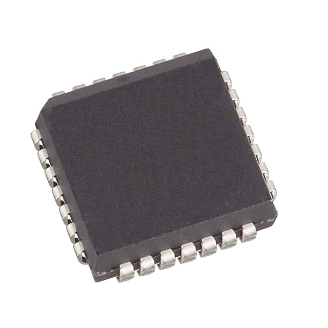
- Part No.:
- DS2182QN+
- Manufacturer:
- Analog Devices Inc./Maxim Integrated
- Category:
- Specialized
- Package:
- 28-LCC (J-Lead)
- Datasheet:
-
 DS2182QN+.pdf
- Description:
- IC MONITOR LINE T1 28-PLCC
- Quantity:
- Payment:

- Shipping:

Inventory:2,230
Please send an inquiry. Send us your inquiry, and we will respond immediately.
Product details
Overview
DS2182QN+ from Maxim Integrated is a T1 line monitor IC designed for real-time performance monitoring in digital telephony infrastructure. It performs framing synchronization (Superframe and Extended Superframe), counts four distinct error types (16-bit bipolar violation, 8-bit CRC, 8-bit OOF, 8-bit frame bit error), detects yellow/blue alarms and carrier loss, and operates from a single 5V supply. It is used in central office line cards and T1 channel banks to maintain service integrity.
For engineers reviewing the DS2182QN+ datasheet, DS2182QN+ pinout, DS2182QN+ application, or DS2182QN+ equivalent, this page delivers verified technical context, exact pin functions, real-world timing roles, and validated alternative parts - all grounded in Maxim's official DS2182A documentation and PLCC packaging specifications.
Technical Context
The DS2182QN+ implements a dual-mode receive synchronizer supporting both 193S (Superframe) and 193E (Extended Superframe) formats, with configurable sync criteria (RCR1.3), sync time (RCR1.2), and auto-resync enable (RCR1.1). Its serial port uses an 8-bit address/command byte with burst mode support and asynchronous register access independent of RCLK timing.
It integrates four dedicated hardware counters - 16-bit BVCR (bipolar violation), and three 8-bit registers (CRCCR, OOFCR, FECR) - each with saturation-triggered interrupt capability and optional auto-reset on read (RCR1.4). Alarm detection includes latched status bits (RSR1/RSR2), maskable interrupts (RIMR1/RIMR2), and direct output pins (RYEL, RLOS, RFER, RBV) synchronized to RCLK.
Key Specifications
| Parameter | Value and Actual Design Meaning |
|---|---|
| Supply Voltage | 5.0 V ±5% - single-supply operation compatible with legacy T1 line card power rails. |
| Data Rate Support | 1.544 MHz - matches standard T1 line rate; RCLK input must be precisely aligned to incoming signal. |
| Framing Modes | 193S (Superframe) and 193E (Extended Superframe) - selectable via RCR2.4; determines CRC usage, F-bit pattern, and alarm detection logic. |
| Error Counters | Four independent hardware counters: 16-bit BVCR, 8-bit CRCCR, 8-bit OOFCR, 8-bit FECR - enable long-duration error accumulation without CPU polling overhead. |
| Alarm Outputs | Dedicated open-drain or push-pull outputs: RYEL (yellow), RLOS (loss-of-sync), RFER (frame error), RBV (bipolar violation) - provide immediate hardware-level fault signaling. |
| Serial Interface | 4-wire SPI-compatible (CS, SCLK, SDI, SDO); supports burst reads/writes and LSB-first data transfer - reduces host controller I/O and initialization time. |
| Operating Temperature | –40°C to +85°C - qualified for industrial and telecom equipment deployed in uncontrolled environments. |
Pinout & Package
DS2182QN+ is housed in a 28-pin Plastic Leaded Chip Carrier (PLCC) package with J-lead configuration, pin-compatible with the DS2182Q variant and mechanically distinct from the DIP versions. The package supports surface-mount assembly and provides thermal and mechanical reliability for telecom-grade PCBs.
| Pin/Terminal | Circuit Role | Design Meaning |
|---|---|---|
| INT | Interrupt Output | Active-low open-drain alarm interrupt; flags host on any enabled condition in RSR1/RSR2. |
| SDI / SDO / CS / SCLK | Serial Port Interface | Full-duplex SPI-like control interface; enables configuration, status readback, and counter access without disrupting T1 monitoring. |
| RCLK | Receive Clock Input | 1.544 MHz primary clock derived from line; drives internal sampling, timing generation, and counter incrementing. |
| RPOS / RNEG | Bipolar Data Inputs | Differential NRZ inputs sampled on falling edge of RCLK; support bipolar violation detection and carrier loss sensing. |
| RLOS / RYEL / RFER / RBV | Real-Time Alarm Outputs | Dedicated status signals - RLOS high during resync, RYEL high on yellow alarm, RFER high on frame bit error, RBV high on bipolar violation. |
| RFSYNC / RMSYNC / RCHCLK | Timing Outputs | Extracted 8 kHz frame sync, 50% duty multiframe sync, and 192 kHz channel clock - enable external demux and signaling extraction. |
| VDD / VSS | Power Supply | 5.0 V supply and signal ground; decoupling required per Maxim layout guidelines to ensure noise immunity on T1 lines. |
Key Features
| Feature | Design Value |
|---|---|
| Superframe & Extended Superframe Support | Hardware-selectable via RCR2.4; eliminates need for firmware rework when upgrading between T1 framing standards. |
| Four Independent Hardware Counters | Enables concurrent long-term error logging (e.g., 16-bit BVCR for >17 hours at 1.544 Mbps) without CPU intervention or memory buffering. |
| Burst Mode Serial Access | Single CS assertion reads/writes all 11 registers; cuts initialization time by >80% vs. discrete register access in embedded systems. |
| Auto Counter Reset on Read | Configurable via RCR1.4; prevents double-counting during polling and ensures accurate delta-error reporting across status updates. |
| Latched Status + Maskable Interrupts | RSR1/RSR2 retain alarm states until read; RIMR1/RIMR2 allow selective disabling of non-critical interrupts (e.g., mask 8ZD while retaining RLOS). |
| Direct Alarm Outputs | RLOS, RYEL, RFER, RBV pins drive LEDs or FPGA inputs directly - bypasses software latency for critical fault response in carrier-grade systems. |
Applications
| Central Office Line Card Monitoring | T1 Channel Bank Health Management |
|---|---|
|
Use Scenario: Real-time supervision of 24 T1 spans in a Class 5 switch environment, where uptime SLAs require sub-second fault detection and isolation. IC Role / Device Role / Timing Role: Primary T1 framing monitor and error accumulator; extracts RFSYNC, RMSYNC, and RCHCLK to synchronize downstream channel processing. Use Value: Reduces mean time to repair (MTTR) by triggering automatic failover upon RLOS or RYEL assertion, while BVCR and FECR logs support root-cause analysis of physical layer degradation. |
Use Scenario: Embedded monitoring in modular T1 channel banks handling 96+ channels, where CPU resources are constrained and deterministic response is mandatory. IC Role / Device Role / Timing Role: Offloads framing alignment, error counting, and alarm generation from host MCU; provides RLINK and RSIGFR for S-bit/ABCD signaling recovery. Use Value: Enables host MCU to poll only once per second via burst mode instead of continuous bit-banging, freeing >30% CPU bandwidth for call control and protocol stack tasks. |
| Remote DSLAM T1 Backhaul Integrity | Legacy PBX T1 Interface Diagnostics |
|
Use Scenario: Unmanned remote DSLAM sites connected via T1 backhaul, where environmental stress causes intermittent carrier loss and framing slips. IC Role / Device Role / Timing Role: Detects RCL (192 consecutive zeros) and COFA (change-of-frame alignment); reports RCLC and RBLC in RSR2 for automated link restoration. Use Value: Eliminates false positives from transient noise by requiring 14+ ones in 112 bits to clear RCL, ensuring stable re-engagement after lightning-induced outages. |
Use Scenario: Field diagnostics for aging PBX systems experiencing increased yellow alarm frequency due to cable aging or impedance mismatch. IC Role / Device Role / Timing Role: Monitors yellow alarm format (193S S-bit or 193E FDL) per RCR2.3/RCR2.4; captures 8ZD/16ZD events to correlate with physical layer issues. Use Value: Provides timestamped 8ZD/16ZD counts alongside RYEL assertions - enabling technicians to distinguish between upstream alarm injection vs. local line degradation. |
Equivalent & Alternatives
The following parts are listed as comparable options for similar T1 line monitor applications.
| Alternative Part | Technical Difference | Application Difference | Selection Advice |
|---|---|---|---|
| DS2182N+ | Same die, 28-pin DIP package; –40°C to +85°C rating identical; no PLCC thermal or mounting advantages. | Preferred for through-hole prototyping or legacy board rework where PLCC reflow is unavailable. | Select DS2182N+ only if DIP footprint and hand-soldering are required; DS2182QN+ offers superior thermal dissipation and board density. |
| DS2175T+ | Single-chip T1 framer/line interface (not monitor-only); lacks BVCR, CRCCR, OOFCR, FECR hardware counters; no RLINK or RSIGFR outputs. | Suitable for endpoint framer applications but cannot replace DS2182QN+ in diagnostic or multi-line monitoring roles. | DS2175T+ is not a functional substitute - it performs framing and HDLC, not passive line monitoring with error accumulation. |
Compared with DS2182N+, DS2182QN+ delivers identical electrical functionality in a surface-mount PLCC package optimized for automated assembly and thermal management; compared with DS2175T+, it provides dedicated monitoring architecture with four hardware error counters and alarm outputs absent in the framer-only device.
Availability
DS2182QN+ is available at Aetrix Electronics and suitable for central office line cards, T1 channel banks, remote DSLAM backhaul, and legacy PBX interface diagnostics requiring stable component supply across extended product lifecycles.
Supply support for DS2182QN+ includes scheduled delivery planning, volume procurement assistance, BOM continuity management, traceable sourcing, and lifecycle availability coordination for OEM customers, industrial embedded developers, connected-device designers, and electronics production programs.
Manufacturer
Maxim Integrated (now part of Analog Devices) is a semiconductor company specializing in precision analog, mixed-signal, and high-reliability interface solutions for communications, industrial, and automotive markets.
The DS2182QN+ belongs to Maxim's T1/E1 line interface and monitoring product line, engineered specifically for carrier-class digital telephony infrastructure where deterministic error detection, low-latency alarm signaling, and long-term statistical monitoring are mission-critical.
FAQ
What is the primary function of the DS2182QN+ in a T1 system?
The DS2182QN+ serves as a dedicated T1 line monitor IC that performs real-time framing synchronization (193S or 193E), accumulates four categories of physical-layer errors (bipolar violations, CRC errors, OOF events, frame bit errors), and generates immediate hardware alarms (RLOS, RYEL, RFER, RBV). It does not perform line driving or framer functions - its role is purely diagnostic and supervisory, enabling robust health monitoring in carrier-grade T1 infrastructure without burdening the host processor.
Does the DS2182QN+ support both Superframe and Extended Superframe formats?
Yes, the DS2182QN+ natively supports both 193S (Superframe) and 193E (Extended Superframe) formats. Selection is controlled by bit RCR2.4: when set to 0, it operates in 193S mode using FT/FS patterns and S-bit detection; when set to 1, it switches to 193E mode using FPS and FDL-based yellow alarm detection with CRC6 validation. This dual-mode capability is implemented in hardware and requires no external components or firmware changes to toggle.
How does the DS2182QN+ handle error counter overflow and interrupt generation?
The DS2182QN+ implements saturation-triggered interrupts for all four counters: the 16-bit BVCR saturates at 65,535 and sets BPVCS in RSR2; the three 8-bit counters (CRCCR, OOFCR, FECR) saturate at 255 and set CRCCS, OOFCS, or FECS respectively. Each saturation bit remains latched until read, and corresponding mask bits in RIMR2 (BPVCS, CRCCS, etc.) enable or disable the associated interrupt on the INT pin - allowing selective alerting based on severity thresholds.
Can the DS2182QN+ be used without a microcontroller?
Yes - the DS2182QN+ provides direct hardware alarm outputs (RLOS, RYEL, RFER, RBV) and timing signals (RFSYNC, RMSYNC, RCHCLK) that can drive LEDs, logic gates, or FPGA inputs without any host processor. While the serial interface enables full configuration and status readback, basic monitoring and fault indication operate autonomously once powered and clocked. The TEST pin must be tied to VSS for normal operation, and RST must be pulsed on power-up to initialize internal state.
What is the significance of the "QN" suffix in DS2182QN+?
The "QN" suffix in DS2182QN+ denotes the 28-pin PLCC package with industrial temperature range (–40°C to +85°C). It distinguishes this variant from DS2182N+ (same temp range, 28-pin DIP) and DS2182Q (0°C to +70°C, 28-pin PLCC). The "+" indicates Maxim's enhanced screening and traceability - confirming compliance with the original DS2182A specification, including B8ZS codeword detection, excessive zero counting (RCR2.5), and SEFE (severely errored framing event) reporting per ANSI T1.231.
DS2182QN+ Specifications
- Product attributes
- Attribute value
- Manufacturer:
- Analog Devices Inc./Maxim Integrated
- Series:
- -
- Package/Case:
- 28-LCC (J-Lead)
- Packaging:
- Tube
- Product Status:
- Obsolete
- Applications:
- Monitors
- Interface:
- Serial
- Voltage - Supply:
- 4.5V ~ 5.5V
- Supplier Device Package:
- 28-PLCC (11.51x11.51)
- Grade:
- -
- Qualification:
- -
- Mounting Type:
- Surface Mount
DS2182QN+ FAQ
1.How can I place an order for DS2182QN+ through Aetrix?
Please submit a Request for Quotation (RFQ) for DS2182QN+ on Aetrix. Our sales agent will provide a competitive quotation and guide you through the order confirmation once you accept the terms.
2.Are the price and stock information for DS2182QN+ reliable?
The price and inventory of DS2182QN+ are updated periodically and may fluctuate due to market conditions. Stock and pricing data are typically refreshed every 24 hours. Quotation validity for DS2182QN+ is usually 5 days.
3.What payment methods are accepted for DS2182QN+?
We accept Wire Transfer, PayPal, Credit Card, Western Union, MoneyGram, and Escrow for DS2182QN+ transactions.
Note: Certain payment methods may incur a processing fee.
4.How is shipping managed for DS2182QN+?
DS2182QN+ orders can be shipped via leading logistics carriers, including DHL, UPS, FedEx, TNT, or Registered Mail.
Once your DS2182QN+ order is processed, you will receive an email with the shipment details and tracking number.
Note: Tracking information may take up to 24 hours to appear. Express delivery typically takes 3–5 business days.
5.How can I obtain technical support or documentation for DS2182QN+?
For technical support, including DS2182QN+ datasheets, pinout diagrams, or application guidance, please contact our engineering support team. They can provide detailed documentation and assistance for your DS2182QN+ requirements.
6.How does Aetrix verify that DS2182QN+ is sourced from the original manufacturer or authorized distributors?
All DS2182QN+ products on Aetrix are procured from qualified distributors and authorized channels. Our dedicated quality assurance team conducts strict verification, including traceability checks and, if necessary, third-party testing. This ensures that DS2182QN+ meets industry standards.
7.What is the process for return or replacement of DS2182QN+?
All DS2182QN+ units undergo pre-shipment inspection (PSI). If there is an issue with DS2182QN+, returns or replacements are accepted under the following conditions:
1.Quantity discrepancies, incorrect items, or visible external defects (such as breakage or corrosion), acknowledged by Aetrix.
2.The issue is reported within 90 days of delivery.
3.The DS2182QN+ part is unused and in its original packaging.
Return procedure for DS2182QN+:
1.Submit a request within 90 days.
2.Obtain a Return Material Authorization (RMA) from Aetrix.
DS2182QN+ Tags

-
NVT4857UKAZ
NXP Semiconductors

-
TCA8418RTWR
Texas Instruments

-
PCA9546APWR
Texas Instruments

-
MD0100N8-G
Microchip Technology

-
PCA9548APW,118
NXP Semiconductors

-
PCA9540BDP,118
NXP Semiconductors

-
PCA9548APWR
Texas Instruments

-
PCA9546APW,118
NXP Semiconductors

-
PTN3360DBS,518
NXP Semiconductors

-
PCA9546ABS,118
NXP Semiconductors

-
PCA9518PWR
Texas Instruments

-
PCA9545APW,118
NXP Semiconductors
Tech Hub

A practical engineering guide to 3.3V and 5V logic compatibility, input thresholds, resistor dividers, translator ICs, MOSFET level shifting, I2C pull-ups, timing limits and power-sequencing risks.

The 74HC595 uses push-pull logic outputs, while the TPIC6B595 uses 50 V open-drain DMOS sinks for higher-power loads. This guide compares timing, current limits, 3.3 V interfacing, load wiring, thermal…

The 74HC595 converts serial data into eight stable parallel outputs. This guide covers pin functions, shift and storage timing, OE and MR behavior, drive-current limits, cascading, voltage compatibilit…

A technical comparison of level-sensitive latches and edge-triggered flip-flops, covering timing windows, setup and hold limits, master–slave operation, time borrowing, race-through, HDL inference and…

A D latch stores one bit while Enable controls when data can pass. This reference covers gate-level operation, truth tables, transparency, setup and hold timing, LE versus OE, common ICs and practical …

An SR latch stores one bit through cross-coupled feedback. This engineering reference covers NOR and NAND implementations, truth tables, forbidden-state recovery, gated operation, switch debouncing, fa…

Latch circuits retain one bit through feedback. This technical reference covers SR and D latches, truth tables, transparency, timing limits, latch-versus-flip-flop behavior, applications and common log…

An engineering guide to LED driver operation, constant-current and constant-voltage outputs, linear and switching topologies, dimming, IC selection, calculations, replacement compatibility, and fault c…

Operational amplifier guide covering op amp basics, feedback, ideal vs real op amps, common configurations, buffer circuits, offset, bias current, gain-bandwidth, slew rate, rail-to-rail limits and sel…

Jumper cables guide covering safe connection order, red and black clamp placement, final ground connection, cable gauge, length, clamp quality, copper vs CCA cables, jump starter comparison and battery…


