
 My Inquiry
 My Account


Analog Devices Inc./Maxim Integrated DS2291/87-22291-000
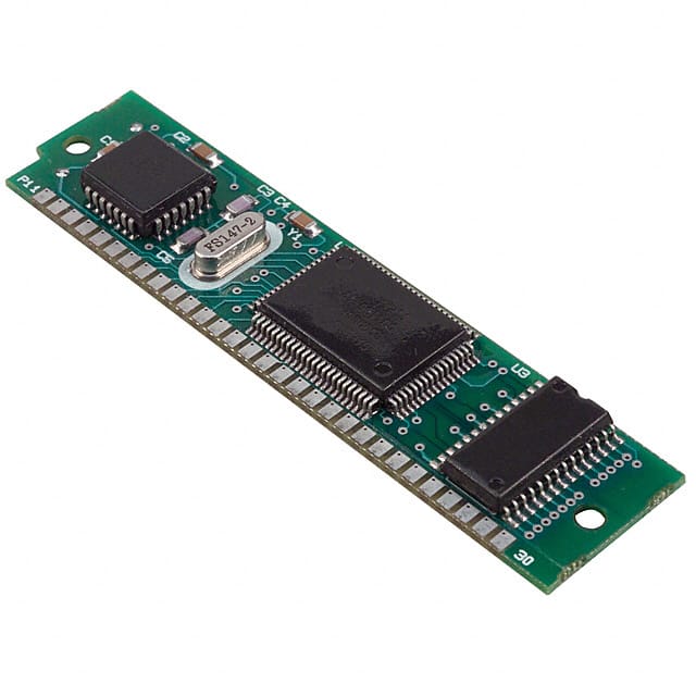
- Part No.:
- DS2291/87-22291-000
- Manufacturer:
- Analog Devices Inc./Maxim Integrated
- Category:
- Specialized
- Package:
- 30-Stik Module
- Datasheet:
-
 DS2291/87-22291-000.pdf
- Description:
- IC INTERFACE SPECIALIZED 30SIP
- Quantity:
- Payment:

- Shipping:

Inventory:4,544
Please send an inquiry. Send us your inquiry, and we will respond immediately.
Product details
Overview
DS2291/87-22291-000 from Maxim Integrated (now part of Analog Devices) is a T1 line interface IC designed for clock and data recovery from long-loop T1 lines up to 6,000 feet. It integrates Automatic Line Build Out (ALBO), jitter attenuation, B8ZS decoding, bipolar violation detection, and carrier loss monitoring - all operating from a single +5V supply and connecting directly to a 30-pin single in-line header. It serves as the core timing recovery engine in Channel Service Units and T1 test equipment.
For engineers reviewing the DS2291/87-22291-000 datasheet, DS2291/87-22291-000 pinout, DS2291/87-22291-000 application, or DS2291/87-22291-000 equivalent, key selection considerations include its TR 62411-compliant jitter tolerance, ALBO adaptation range (0–6,000 ft), 1.544 MHz recovered clock output, B8ZS enable control, and lock-status indication via the LOCK pin.
Technical Context
The DS2291/87-22291-000 implements analog front-end conditioning with a 1100 Ω input impedance at 772 kHz and –30 to 0 dBSX receiver sensitivity, enabling robust signal acquisition across varying line lengths. Its ALBO circuit dynamically adjusts gain and equalization without external tuning components, while the integrated dejitter circuitry provides frequency-dependent attenuation per TR 62411 Curve A/B up to 100 kHz.
Digital functionality includes a 128-bit recenterable buffer, loopback mux control (LB pin), and real-time status reporting via dedicated open-drain outputs: LOCK (phase/frequency lock), BPV (bipolar violation), RCL (carrier loss), and BL (buffer limit at >120 UIpp jitter). All digital I/Os are TTL-compatible except LCLK/LPOS/LNEG, which require HC-level thresholds.
Key Specifications
| Parameter | Value and Actual Design Meaning |
|---|---|
| Recovery Rate | 1.544 MHz T1 line rate; delivers synchronized RCLK, RPOS, RNEG outputs aligned to incoming signal. |
| Line Length Support | 0–6,000 ft via integrated ALBO; eliminates manual gain/equalization adjustments for field deployment. |
| Jitter Attenuation | Meets TR 62411 Curve A/B; reduces input jitter ≥20 dB at 100 Hz–100 kHz when DJA = low. |
| Receiver Sensitivity | –30 to 0 dBSX (3 Vpk reference); accommodates wide dynamic range of transformer-coupled T1 signals. |
| Supply Voltage | +4.75 V to +5.25 V; single-rail operation simplifies power design in CSU and test equipment. |
| Operating Temp | 0°C to +70°C; validated for commercial-grade telecom infrastructure applications. |
| Input Impedance | 1100 Ω at 772 kHz; matches standard T1 line interface requirements with 2:1 transformer coupling. |
Pinout & Package
DS2291/87-22291-000 is housed in a through-hole 30-pin single in-line (SIL) package with 0.100" pin spacing, compatible with standard SIL headers used in CSUs and test fixtures. Pin 1 (VDD) is marked by a notch on the package body.
| Pin/Terminal | Circuit Role | Design Meaning |
|---|---|---|
| VDD (Pins 1,2) | Power Supply Input | +5 V supply pins; decoupling required near pin 1 for stable ALBO and dejitter operation. |
| RX+, RX– (Pins 29,30) | Differential Analog Input | Connects to secondary of 2:1 transformer; accepts –30 to 0 dBSX T1 signal with 1100 Ω impedance match. |
| RCLK, RPOS, RNEG (Pins 3–5) | Recovered Clock & Data Outputs | 1.544 MHz clock and bipolar data outputs referenced to RCLK rising edge; drive TTL loads. |
| LOCK (Pin 16) | Status Output | Active-high open-drain indicator confirming phase/frequency lock to incoming T1 signal. |
| B8ZS (Pin 20) | Control Input | Tie high to decode and replace B8ZS code words with eight zeros; tie low/open for raw bipolar output. |
| DJA (Pin 19) | Control Input | Tie low to enable TR 62411-compliant jitter attenuation; tie high to bypass dejitter circuitry. |
| BL (Pin 17) | Status Output | Active-high open-drain flag indicating >120 UIpp peak-to-peak jitter at RX+/RX– inputs. |
Key Features
| Feature | Design Value |
|---|---|
| Integrated ALBO | Adapts gain and equalization automatically across 0–6,000 ft T1 line lengths - no external tuning components or calibration required. |
| TR 62411 Compliance | Fully meets jitter tolerance and attenuation specifications per AT&T TR 62411 (Dec. 1990), including Curve A/B performance. |
| Real-Time Status Monitoring | Dedicated open-drain outputs (LOCK, BPV, RCL, BL) provide immediate fault visibility without software polling. |
| B8ZS Code Handling | Selectable B8ZS decoding and zero-substitution via B8ZS pin - supports both legacy and modern T1 framing schemes. |
| Loopback Mux Architecture | LB-controlled data routing enables local/remote loopback testing for system diagnostics and fault isolation. |
Applications
| Channel Service Unit (CSU) | T1 Test Equipment |
|---|---|
Use Scenario: Installed in carrier-class CSUs to recover clock and data from long-haul T1 lines with variable impedance and loss. IC Role / Device Role / Timing Role: Primary T1 line interface IC performing ALBO-based signal conditioning, jitter cleanup, and B8ZS-aware data recovery. Use Value: Eliminates need for manual line equalization and external jitter cleaners, reducing bill-of-materials and field maintenance. |
Use Scenario: Embedded in portable T1 analyzers and bit-error-rate testers for lab and field validation of T1 line integrity. IC Role / Device Role / Timing Role: Core signal recovery engine providing lock status, BPV detection, and carrier loss alerts for real-time diagnostics. Use Value: Enables rapid identification of line faults (e.g., opens, shorts, excessive jitter) via dedicated status pins without host processor intervention. |
| T1 Monitoring Systems | Network Interface Cards |
Use Scenario: Deployed in central office monitoring systems tracking uptime, error rates, and signal quality across multiple T1 feeds. IC Role / Device Role / Timing Role: Standalone T1 receiver feeding recovered clock/data into FPGA-based frame synchronizers and error counters. Use Value: Provides deterministic jitter attenuation and reliable lock detection - critical for accurate BER measurement over extended periods. |
Use Scenario: Used in enterprise-grade WAN interface cards requiring T1 connectivity with FCC Part 68 compliance via companion DS2290 isolation. IC Role / Device Role / Timing Role: Timing recovery block interfacing with DS2290 Isolation Stik and DS2180A transceiver in protected line interface designs. Use Value: Enables safe, surge-protected T1 termination while maintaining full ALBO adaptability and TR 62411-compliant jitter performance. |
Equivalent & Alternatives
The following parts are listed as comparable options for similar T1 line interface applications.
| Alternative Part | Technical Difference | Application Difference | Selection Advice |
|---|---|---|---|
| DS2290 | Isolation-focused companion device; lacks ALBO, dejitter, and B8ZS decode - provides only transformer-coupled protection and level shifting. | Used upstream of DS2291/87-22291-000 for FCC Part 68 compliance; not a functional substitute. | Select DS2290 only when galvanic isolation and surge protection are required - it must be paired with DS2291/87-22291-000 or similar recovery IC. |
| DS2180A | Full-duplex T1 transceiver; includes line driver, receiver, and framing logic - but no ALBO, dejitter, or B8ZS handling. | Designed for complete T1 PHY layer implementation; requires external clock recovery and jitter cleanup stages. | Choose DS2180A when building end-to-end T1 transceivers; use DS2291/87-22291-000 when only high-fidelity clock/data recovery from long loops is needed. |
Compared with DS2290 and DS2180A, the DS2291/87-22291-000 uniquely combines adaptive line build-out, TR 62411-compliant jitter attenuation, and B8ZS-aware signal recovery in a single 30-pin SIL package - making it irreplaceable for long-loop T1 monitoring and CSU applications where signal integrity and autonomous adaptation are critical.
Availability
DS2291/87-22291-000 is available at Aetrix Electronics and suitable for Channel Service Units, T1 test equipment, and network monitoring systems requiring stable component supply, long-term lifecycle support, and traceable sourcing for telecom infrastructure programs.
Supply support for DS2291/87-22291-000 includes scheduled delivery planning, volume procurement assistance, BOM continuity management, traceable sourcing, and lifecycle availability coordination for OEM customers, industrial embedded developers, connected-device designers, and electronics production programs.
Manufacturer
Maxim Integrated (acquired by Analog Devices in 2021) is a semiconductor company specializing in precision analog, mixed-signal, and power management ICs for communications, industrial, and computing applications.
The DS2291/87-22291-000 belongs to Maxim's T1/E1 interface product line, engineered specifically for carrier-grade line interface units requiring autonomous signal recovery, jitter mitigation, and standards-compliant diagnostics in unconditioned loop environments.
FAQ
What is the primary function of the DS2291/87-22291-000 in a T1 system?
The DS2291/87-22291-000 functions as a T1 line interface IC that recovers clock and bipolar data from long-loop T1 lines up to 6,000 feet. It performs automatic line build out (ALBO), jitter attenuation per TR 62411, B8ZS decoding, bipolar violation detection, and carrier loss monitoring - all within a single +5V-powered 30-pin SIL package. The DS2291/87-22291-000 delivers synchronized RCLK, RPOS, and RNEG outputs essential for downstream frame synchronization and error analysis.
How does the ALBO circuit in the DS2291/87-22291-000 adapt to different T1 line lengths?
The DS2291/87-22291-000 ALBO circuit dynamically adjusts gain and equalization in real time to compensate for signal loss across T1 line lengths from 0 to 6,000 feet - without requiring external tuning components or manual calibration. This adaptation ensures consistent receiver sensitivity (–30 to 0 dBSX) and reliable lock acquisition regardless of line impedance or distance. The DS2291/87-22291-000 achieves this using internal feedback loops that monitor signal integrity and adjust analog front-end parameters autonomously.
What does the LOCK pin indicate, and how is it used in system design?
On the DS2291/87-22291-000, the LOCK pin is an active-high open-drain output that signals successful phase-and-frequency lock to the incoming T1 signal. When high, it confirms stable 1.544 MHz clock recovery and valid data alignment at RPOS/RNEG. System designers use this pin for hardware-level status monitoring, fault detection, and automatic failover - for example, disabling downstream processing until LOCK asserts. The DS2291/87-22291-000 guarantees LOCK assertion only after meeting TR 62411 jitter tolerance criteria.
Can the DS2291/87-22291-000 handle B8ZS-encoded T1 signals, and how is it configured?
Yes, the DS2291/87-22291-000 supports B8ZS-encoded T1 signals via the B8ZS pin (Pin 20). When tied high, it decodes B8ZS code words and replaces them with eight consecutive zeros; when tied low or left open, it passes raw bipolar data without modification. Bipolar violations (BPV) are reported independently via the BPV pin, though BPV detection is disabled during B8ZS decoding. This configuration allows the DS2291/87-22291-000 to interoperate with both legacy AMI and modern B8ZS-framed T1 networks.
What is the purpose of the DJA pin, and what happens when it is asserted high?
The DJA (Disable Jitter Attenuation) pin on the DS2291/87-22291-000 controls activation of the integrated dejitter circuitry. When DJA is tied low (default), the DS2291/87-22291-000 applies TR 62411-compliant attenuation across 100 Hz–100 kHz. When DJA is tied high, jitter attenuation is fully bypassed - passing all input jitter directly to RCLK, RPOS, and RNEG. This mode is used only when downstream circuitry handles jitter cleanup, but the DS2291/87-22291-000 datasheet recommends keeping DJA low for most T1 transmission applications.
DS2291/87-22291-000 Specifications
- Product attributes
- Attribute value
- Manufacturer:
- Analog Devices Inc./Maxim Integrated
- Series:
- -
- Package/Case:
- 30-Stik Module
- Packaging:
- Bulk
- Product Status:
- Obsolete
- Applications:
- Data Transport
- Interface:
- -
- Voltage - Supply:
- 5V
- Supplier Device Package:
- -
- Grade:
- -
- Qualification:
- -
- Mounting Type:
- Surface Mount
DS2291/87-22291-000 FAQ
1.How can I place an order for DS2291/87-22291-000 through Aetrix?
Please submit a Request for Quotation (RFQ) for DS2291/87-22291-000 on Aetrix. Our sales agent will provide a competitive quotation and guide you through the order confirmation once you accept the terms.
2.Are the price and stock information for DS2291/87-22291-000 reliable?
The price and inventory of DS2291/87-22291-000 are updated periodically and may fluctuate due to market conditions. Stock and pricing data are typically refreshed every 24 hours. Quotation validity for DS2291/87-22291-000 is usually 5 days.
3.What payment methods are accepted for DS2291/87-22291-000?
We accept Wire Transfer, PayPal, Credit Card, Western Union, MoneyGram, and Escrow for DS2291/87-22291-000 transactions.
Note: Certain payment methods may incur a processing fee.
4.How is shipping managed for DS2291/87-22291-000?
DS2291/87-22291-000 orders can be shipped via leading logistics carriers, including DHL, UPS, FedEx, TNT, or Registered Mail.
Once your DS2291/87-22291-000 order is processed, you will receive an email with the shipment details and tracking number.
Note: Tracking information may take up to 24 hours to appear. Express delivery typically takes 3–5 business days.
5.How can I obtain technical support or documentation for DS2291/87-22291-000?
For technical support, including DS2291/87-22291-000 datasheets, pinout diagrams, or application guidance, please contact our engineering support team. They can provide detailed documentation and assistance for your DS2291/87-22291-000 requirements.
6.How does Aetrix verify that DS2291/87-22291-000 is sourced from the original manufacturer or authorized distributors?
All DS2291/87-22291-000 products on Aetrix are procured from qualified distributors and authorized channels. Our dedicated quality assurance team conducts strict verification, including traceability checks and, if necessary, third-party testing. This ensures that DS2291/87-22291-000 meets industry standards.
7.What is the process for return or replacement of DS2291/87-22291-000?
All DS2291/87-22291-000 units undergo pre-shipment inspection (PSI). If there is an issue with DS2291/87-22291-000, returns or replacements are accepted under the following conditions:
1.Quantity discrepancies, incorrect items, or visible external defects (such as breakage or corrosion), acknowledged by Aetrix.
2.The issue is reported within 90 days of delivery.
3.The DS2291/87-22291-000 part is unused and in its original packaging.
Return procedure for DS2291/87-22291-000:
1.Submit a request within 90 days.
2.Obtain a Return Material Authorization (RMA) from Aetrix.
DS2291/87-22291-000 Tags

-
NVT4857UKAZ
NXP Semiconductors

-
TCA8418RTWR
Texas Instruments

-
PCA9546APWR
Texas Instruments

-
MD0100N8-G
Microchip Technology

-
PCA9548APW,118
NXP Semiconductors

-
PCA9540BDP,118
NXP Semiconductors

-
PCA9548APWR
Texas Instruments

-
PCA9546APW,118
NXP Semiconductors

-
PTN3360DBS,518
NXP Semiconductors

-
PCA9546ABS,118
NXP Semiconductors

-
PCA9518PWR
Texas Instruments

-
PCA9545APW,118
NXP Semiconductors
Tech Hub

A practical engineering guide to 3.3V and 5V logic compatibility, input thresholds, resistor dividers, translator ICs, MOSFET level shifting, I2C pull-ups, timing limits and power-sequencing risks.

The 74HC595 uses push-pull logic outputs, while the TPIC6B595 uses 50 V open-drain DMOS sinks for higher-power loads. This guide compares timing, current limits, 3.3 V interfacing, load wiring, thermal…

The 74HC595 converts serial data into eight stable parallel outputs. This guide covers pin functions, shift and storage timing, OE and MR behavior, drive-current limits, cascading, voltage compatibilit…

A technical comparison of level-sensitive latches and edge-triggered flip-flops, covering timing windows, setup and hold limits, master–slave operation, time borrowing, race-through, HDL inference and…

A D latch stores one bit while Enable controls when data can pass. This reference covers gate-level operation, truth tables, transparency, setup and hold timing, LE versus OE, common ICs and practical …

An SR latch stores one bit through cross-coupled feedback. This engineering reference covers NOR and NAND implementations, truth tables, forbidden-state recovery, gated operation, switch debouncing, fa…

Latch circuits retain one bit through feedback. This technical reference covers SR and D latches, truth tables, transparency, timing limits, latch-versus-flip-flop behavior, applications and common log…

An engineering guide to LED driver operation, constant-current and constant-voltage outputs, linear and switching topologies, dimming, IC selection, calculations, replacement compatibility, and fault c…

Operational amplifier guide covering op amp basics, feedback, ideal vs real op amps, common configurations, buffer circuits, offset, bias current, gain-bandwidth, slew rate, rail-to-rail limits and sel…

Jumper cables guide covering safe connection order, red and black clamp placement, final ground connection, cable gauge, length, clamp quality, copper vs CCA cables, jump starter comparison and battery…


