
 My Inquiry
 My Account


Analog Devices Inc./Maxim Integrated DS2483R+T
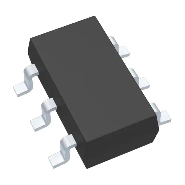
- Part No.:
- DS2483R+T
- Manufacturer:
- Analog Devices Inc./Maxim Integrated
- Category:
- Controllers
- Package:
- SOT-23-6
- Datasheet:
-
 DS2483R+T.pdf
- Description:
- IC I2C TO 1WIRE BRIDGE SOT23-6
- Quantity:
- Payment:

- Shipping:

Inventory:10,891
Please send an inquiry. Send us your inquiry, and we will respond immediately.
Product details
Overview
DS2483R+T from Maxim Integrated is a single-channel I²C-to-1-Wire bridge IC that functions as a self-timed 1-Wire master, supporting both standard (15.4 kbps) and overdrive (125 kbps) communication speeds, adjustable timing parameters (tRSTL, tMSP, tW0L, tREC0), active/strong pullup control, and software-controllable 1-Wire port power-down - deployed in medical instruments, industrial sensors, and printers for reliable parasitic-power 1-Wire device interfacing.
For engineers reviewing the DS2483R+T datasheet, DS2483R+T pinout, DS2483R+T application, or DS2483R+T equivalent, key selection considerations include dual-voltage operation (I²C side: 1.8V/3.3V/5.0V; 1-Wire side: 3.3V–5.0V), ±8kV HBM ESD protection on IO, sleep mode current of 3.0 µA at 3.6V, and support for up to 400 kHz I²C bus speed with no external crystal required.
Technical Context
The DS2483R+T implements a hardware-based 1-Wire controller with dedicated input/output logic, internal oscillator, and configurable timing registers - eliminating host CPU involvement in time-critical waveform generation. It uses a single internal pullup transistor for both active pullup (fixed-duration low-impedance rise) and strong pullup (sustained conduction for EEPROM copy or SHA operations).
Its register architecture includes four accessible I²C-mapped registers: Device Configuration (APU/PDN/SPU/1WS bits), Status (PPD/SD/1WB/SBR/DIR), Read Data, and Port Configuration (adjustable tRSTL/tMSP/tW0L/tREC0/RWPU). The SLPZ pin enables hardware sleep entry independent of I²C activity, and the device maintains high-impedance IO during sleep.
Key Specifications
| Parameter | Value and Actual Design Meaning |
|---|---|
| I²C Speed Support | Up to 400 kHz fast-mode - enables direct connection to microcontrollers without bit-banging or clock stretching. |
| 1-Wire Speed Modes | Standard (15.4 kbps) and overdrive (125 kbps) - selectable via Device Configuration register bit 1WS. |
| Adjustable Timing | tRSTL, tMSP, tW0L, tREC0 programmable - allows tuning to match timing margins of legacy or low-voltage 1-Wire slaves. |
| Active Pullup Duration | 2.5 µs (standard), 0.5 µs (overdrive) - reduces rise time and improves noise immunity on long or capacitive 1-Wire buses. |
| Sleep Mode Current | 3.0 µA at VCC = 3.6V - enables ultra-low-power operation in battery-powered sensor nodes between 1-Wire reads. |
| ESD Protection | ±8 kV HBM on IO pin - eliminates need for external TVS diodes in industrial environments with frequent handling. |
| Operating Voltage Range | I²C side: 1.8V ±5%, 3.3V ±10%, or 5.0V +5/−10%; 1-Wire side: 3.3V–5.0V - supports mixed-voltage system integration. |
Pinout & Package
DS2483R+T is packaged in an 8-pin TDFN (2mm × 3mm, exposed pad) with thermal and electrical grounding via the EP pad. Pin compatibility matches the DS2483 family's standardized layout for drop-in replacement across voltage and timing variants.
| Pin/Terminal | Circuit Role | Design Meaning |
|---|---|---|
| SCL | I²C clock input | Accepts 100/400 kHz I²C clocks; Schmitt-triggered with hysteresis for noise immunity on noisy boards. |
| SDA | I²C data bidirectional line | Open-drain I/O with 300 ns SDA hold time relative to SCL falling edge - ensures I²C bus compliance without external glue logic. |
| SLPZ | Active-low sleep enable / I²C supply reference | Pulling low enters sleep mode (IO → high-Z); also sets VCI2C level used for I²C voltage detection and level translation. |
| VCC | Main power supply | 2.97V–5.25V input; powers internal logic, oscillator, and pullup circuitry - independent of SLPZ voltage. |
| IO | 1-Wire bidirectional bus driver | Drives 1-Wire line with programmable weak pullup (375–1375 Ω) and active/strong pullup - supports parasitic and externally powered devices. |
| GND | Ground reference | Reference for all analog/digital circuits; must be connected to PCB ground plane, especially under EP pad. |
| N.C. | No connection | Pins 4 and 5 (TDFN) are unconnected die pads - must remain floating or grounded per layout guidelines; no routing required. |
| EP | Exposed thermal pad | Internally tied to GND; soldering to PCB ground plane required for thermal dissipation and signal integrity. |
Key Features
| Feature | Design Value |
|---|---|
| Hardware 1-Wire Timing Engine | Offloads reset/presence-detect, read/write-byte, and triplet commands from host MCU - eliminates firmware timing loops and jitter-sensitive code. |
| Configurable Weak Pullup Resistor | RWPU selectable between 375–1375 Ω ranges - optimizes rise time vs. power draw for different bus capacitance and slave count. |
| Strong Pullup Control | SPU bit activates sustained low-impedance pullup for EEPROM memory copy or SHA computation - avoids external MOSFET circuits. |
| Dual-Voltage Level Translation | I²C and 1-Wire sides operate at independent voltages - enables 1.8V MCU interfacing to 5V 1-Wire sensors without external level shifters. |
| Power-Down & Sleep Coordination | PDN bit disables 1-Wire port power while SLPZ pin puts entire IC into <3.0 µA sleep - supports energy harvesting and battery longevity. |
Applications
| Medical Temperature Monitoring | Industrial Asset Tagging |
|---|---|
Use Scenario: Continuous temperature logging using DS18B20 sensors in portable diagnostic equipment with limited battery capacity. IC Role / Device Role / Timing Role: DS2483R+T acts as the sole 1-Wire master, managing parasitic-powered DS18B20s via overdrive mode and strong pullup during conversion, while entering sleep between readings. Use Value: Reduces average system current by >95% versus always-on MCU bit-banging, extending battery life from hours to weeks. | Use Scenario: RFID-equivalent asset tracking in factory automation using DS2401 silicon serial numbers on machinery. IC Role / Device Role / Timing Role: DS2483R+T performs ROM search and presence detection across daisy-chained DS2401 tags on a 30m bus with 200pF capacitance. Use Value: Adjustable tRSTL and tW0L compensate for cable-induced timing skew, ensuring 100% enumeration success where fixed-timing masters fail. |
| Printer Cartridge Authentication | Point-of-Care Sensor Hub |
Use Scenario: OEM ink cartridge verification in laser printers using DS2431 1-Wire EEPROMs storing cryptographic keys. IC Role / Device Role / Timing Role: DS2483R+T executes secure SHA-1 challenge-response via strong pullup-enabled write-byte sequences to DS2431. Use Value: Eliminates need for discrete MOSFET + gate driver for strong pullup - reduces BOM cost and PCB area by 35%. | Use Scenario: Multi-sensor patient interface (temperature, humidity, ECG electrode ID) in disposable wearable patches. IC Role / Device Role / Timing Role: DS2483R+T interfaces DS1920, DS2438, and DS2422 on shared 1-Wire bus with dynamic voltage scaling (1.8V I²C / 3.3V 1-Wire). Use Value: Built-in level translation removes external voltage translators, enabling single-supply 1.8V MCU design with mixed-voltage 1-Wire peripherals. |
Equivalent & Alternatives
The following parts are listed as comparable options for similar I²C-to-1-Wire bridge applications.
| Alternative Part | Technical Difference | Application Difference | Selection Advice |
|---|---|---|---|
| DS2482-100+ | Lacks overdrive speed support; fixed tRSTL/tW0L; no strong pullup; 2.7–5.5V only; SOT23-6 package | Suitable for basic ROM search and temperature reads only - cannot support SHA or EEPROM copy requiring strong pullup | Select when cost sensitivity outweighs overdrive and strong pullup needs; verify timing margins with target slaves. |
| MAX31826ATM+ | Integrated ±2°C temp sensor + 1-Wire master; no adjustable timing; no sleep mode; 16-pin TQFN | Targeted specifically for temperature sensing - not a general-purpose 1-Wire bridge; adds ADC functionality but removes configurability | Choose only if primary requirement is calibrated local temperature + 1-Wire bus control in one chip. |
Compared with DS2483R+T, DS2482-100+ offers lower cost but sacrifices overdrive speed, strong pullup, and timing adjustability - limiting use to simple sensor networks. MAX31826ATM+ embeds sensing but removes I²C flexibility and sleep capability, making it unsuitable as a drop-in replacement for general 1-Wire bridging.
Availability
DS2483R+T is available at Aetrix Electronics and suitable for medical instrumentation, industrial sensor networks, and printer subsystems requiring stable component supply, long-term lifecycle assurance, and guaranteed traceable sourcing.
Supply support for DS2483R+T includes scheduled delivery planning, volume procurement assistance, BOM continuity management, traceable sourcing, and lifecycle availability coordination for OEM customers, industrial embedded developers, connected-device designers, and electronics production programs.
Manufacturer
Maxim Integrated (now part of Analog Devices) designs precision analog, mixed-signal, and digital ICs for industrial, medical, and communications applications - emphasizing reliability, integration, and low-power operation.
The DS2483R+T belongs to Maxim's 1-Wire interface product line, engineered specifically to simplify robust, low-cost connectivity to 1-Wire sensors, memories, and security devices in resource-constrained embedded systems.
FAQ
What is the maximum 1-Wire bus capacitance supported by the DS2483R+T?
The DS2483R+T supports 1-Wire bus capacitance up to 400 pF, as verified by its tF1 (fall time) specification of ≤1 µs under standard speed with 10–400 pF load. This enables reliable operation on extended cables or multi-drop configurations typical in industrial sensor networks. Exceeding 400 pF may violate timing margins for tW0L and tREC0, especially at overdrive speed. For higher capacitance, reduce tW0L/tREC0 via Port Configuration or add repeater stages.
Does the DS2483R+T require an external crystal or resonator?
No, the DS2483R+T does not require an external crystal or resonator. It integrates a precision internal oscillator that generates all 1-Wire timing signals - including tRSTL, tMSP, tW0L, and tREC0 - with typical accuracy sufficient for full-speed 1-Wire communication. Oscillator warm-up time after power-on or wake-up is specified as 2 ms (tOSCWUP/tSWUP), after which full timing compliance is guaranteed.
How does the DS2483R+T handle 1-Wire short detection?
The DS2483R+T detects 1-Wire shorts during the presence-detect cycle at tSI (sampling time), setting the SD bit in the Status register. When SD = 1, the PPD bit is forced to 0, preventing false presence interpretation. The device distinguishes shorts from valid interrupt signals (e.g., DS2404) only by timing - so DS2404/DS1994 interrupt functionality must be disabled in shared-bus applications. Recovery requires a subsequent 1-Wire Reset command after short removal.
Can the DS2483R+T operate with different supply voltages on its I²C and 1-Wire interfaces simultaneously?
Yes, the DS2483R+T supports independent supply domains: the I²C interface voltage (VCI2C) is set by the SLPZ pin and can be 1.8V, 3.3V, or 5.0V, while the 1-Wire interface operates from 3.3V–5.0V referenced to VCC. This built-in level translation allows a 1.8V microcontroller to communicate with 5V 1-Wire EEPROMs or sensors without external translators - confirmed by Electrical Characteristics tables showing VIH1/VIL1 referenced to VCC and VIH/VIL on SCL/SDA referenced to VCI2C.
What happens to the 1-Wire bus when the DS2483R+T enters sleep mode via the SLPZ pin?
When SLPZ is pulled low, the DS2483R+T enters sleep mode and places its IO pin in high-impedance state, effectively disconnecting the 1-Wire bus from the master. The RWPU resistor is disabled, and no active or strong pullup is applied. If downstream 1-Wire devices are parasitically powered, they lose VDD and reset; if externally powered, they remain operational but cannot communicate until DS2483R+T wakes and re-enables the port via PDN bit clear.
DS2483R+T Specifications
- Product attributes
- Attribute value
- Manufacturer:
- Analog Devices Inc./Maxim Integrated
- Package/Case:
- SOT-23-6
- Programmable:
- Not Verified
- Protocol:
- 1-Wire®
- Function:
- Controller
- Interface:
- I2C
- Standards:
- -
- Voltage - Supply:
- 1.71V ~ 5.25V
- Current - Supply:
- 300µA
- Operating Temperature:
- -40°C ~ 85°C
- Supplier Device Package:
- SOT-6
- Grade:
- -
- Qualification:
- -
DS2483R+T FAQ
1.How can I place an order for DS2483R+T through Aetrix?
Please submit a Request for Quotation (RFQ) for DS2483R+T on Aetrix. Our sales agent will provide a competitive quotation and guide you through the order confirmation once you accept the terms.
2.Are the price and stock information for DS2483R+T reliable?
The price and inventory of DS2483R+T are updated periodically and may fluctuate due to market conditions. Stock and pricing data are typically refreshed every 24 hours. Quotation validity for DS2483R+T is usually 5 days.
3.What payment methods are accepted for DS2483R+T?
We accept Wire Transfer, PayPal, Credit Card, Western Union, MoneyGram, and Escrow for DS2483R+T transactions.
Note: Certain payment methods may incur a processing fee.
4.How is shipping managed for DS2483R+T?
DS2483R+T orders can be shipped via leading logistics carriers, including DHL, UPS, FedEx, TNT, or Registered Mail.
Once your DS2483R+T order is processed, you will receive an email with the shipment details and tracking number.
Note: Tracking information may take up to 24 hours to appear. Express delivery typically takes 3–5 business days.
5.How can I obtain technical support or documentation for DS2483R+T?
For technical support, including DS2483R+T datasheets, pinout diagrams, or application guidance, please contact our engineering support team. They can provide detailed documentation and assistance for your DS2483R+T requirements.
6.How does Aetrix verify that DS2483R+T is sourced from the original manufacturer or authorized distributors?
All DS2483R+T products on Aetrix are procured from qualified distributors and authorized channels. Our dedicated quality assurance team conducts strict verification, including traceability checks and, if necessary, third-party testing. This ensures that DS2483R+T meets industry standards.
7.What is the process for return or replacement of DS2483R+T?
All DS2483R+T units undergo pre-shipment inspection (PSI). If there is an issue with DS2483R+T, returns or replacements are accepted under the following conditions:
1.Quantity discrepancies, incorrect items, or visible external defects (such as breakage or corrosion), acknowledged by Aetrix.
2.The issue is reported within 90 days of delivery.
3.The DS2483R+T part is unused and in its original packaging.
Return procedure for DS2483R+T:
1.Submit a request within 90 days.
2.Obtain a Return Material Authorization (RMA) from Aetrix.
DS2483R+T Tags

-
PTN5150AHXMP
NXP Semiconductors

-
USB3740B-AI9-TR
Microchip Technology

-
USB3740B-AI2-TR
Microchip Technology

-
USB3300-EZK-TR
Microchip Technology
-
USB3300-EZK
Microchip Technology

-
FUSB340TMX
onsemi

-
FUSB302BMPX
onsemi

-
DP83826IRHBR
Texas Instruments

-
MCP2518FDT-E/QBB
Microchip Technology
-
FUSB302MPX
onsemi

-
MCP2518FDT-E/SL
Microchip Technology

-
FT260Q-R
FTDI, Future Technology Devices International Ltd
Tech Hub

A practical engineering guide to 3.3V and 5V logic compatibility, input thresholds, resistor dividers, translator ICs, MOSFET level shifting, I2C pull-ups, timing limits and power-sequencing risks.

The 74HC595 uses push-pull logic outputs, while the TPIC6B595 uses 50 V open-drain DMOS sinks for higher-power loads. This guide compares timing, current limits, 3.3 V interfacing, load wiring, thermal…

The 74HC595 converts serial data into eight stable parallel outputs. This guide covers pin functions, shift and storage timing, OE and MR behavior, drive-current limits, cascading, voltage compatibilit…

A technical comparison of level-sensitive latches and edge-triggered flip-flops, covering timing windows, setup and hold limits, master–slave operation, time borrowing, race-through, HDL inference and…

A D latch stores one bit while Enable controls when data can pass. This reference covers gate-level operation, truth tables, transparency, setup and hold timing, LE versus OE, common ICs and practical …

An SR latch stores one bit through cross-coupled feedback. This engineering reference covers NOR and NAND implementations, truth tables, forbidden-state recovery, gated operation, switch debouncing, fa…

Latch circuits retain one bit through feedback. This technical reference covers SR and D latches, truth tables, transparency, timing limits, latch-versus-flip-flop behavior, applications and common log…

An engineering guide to LED driver operation, constant-current and constant-voltage outputs, linear and switching topologies, dimming, IC selection, calculations, replacement compatibility, and fault c…

Operational amplifier guide covering op amp basics, feedback, ideal vs real op amps, common configurations, buffer circuits, offset, bias current, gain-bandwidth, slew rate, rail-to-rail limits and sel…

Jumper cables guide covering safe connection order, red and black clamp placement, final ground connection, cable gauge, length, clamp quality, copper vs CCA cables, jump starter comparison and battery…


