
 My Inquiry
 My Account


Analog Devices Inc./Maxim Integrated DS24B33Q+T&R
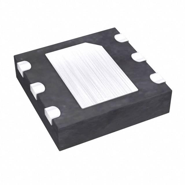
- Part No.:
- DS24B33Q+T&R
- Manufacturer:
- Analog Devices Inc./Maxim Integrated
- Category:
- Memory
- Package:
- 6-WDFN Exposed Pad
- Datasheet:
-
 DS24B33Q+T&R.pdf
- Description:
- IC EEPROM 4KBIT 1-WIRE 6TDFN
- Quantity:
- Payment:

- Shipping:

Inventory:10,981
Please send an inquiry. Send us your inquiry, and we will respond immediately.
Product details
Overview
DS24B33Q+T&R from Analog Devices is a 4096-bit, 1-Wire® EEPROM organized as sixteen 256-bit memory pages, featuring a 32-byte scratchpad for verified write operations, 64-bit unique factory-programmed registration number, and parasitic power operation over a single-conductor bus. It operates from +2.8V to +5.25V across –40°C to +85°C and supports 15.4kbps/125kbps communication speeds - used for calibration constant storage, PCB identification, and product revision tracking in industrial sensor nodes and embedded systems.
For engineers reviewing the DS24B33Q+T&R datasheet, DS24B33Q+T&R pinout, DS24B33Q+T&R application, or DS24B33Q+T&R equivalent, key selection considerations include its TDFN-EP (3mm × 3mm) package with exposed pad grounding requirement, 200k write/erase cycles at +25°C, 40-year data retention at +85°C, open-drain IO interface with programmable hysteresis, and strict backward compatibility with DS2433 ROM command set and memory addressing.
Technical Context
The DS24B33Q+T&R implements a parasitically powered 1-Wire slave architecture with no VCC pin - all operating energy drawn from the IO line during high-time slots. Its internal circuitry includes a CRC-16 generator for ROM and memory command integrity, dedicated address registers (TA1/TA2/E/S), and automatic scratchpad-to-EEPROM copy logic triggered only upon exact 3-byte authorization pattern match.
Communication follows the standard 1-Wire protocol hierarchy: ROM function commands (e.g., Match ROM, Skip ROM) must precede memory functions (Write Scratchpad, Copy Scratchpad, Read Memory); overdrive mode enables 125kbps operation after Overdrive-Skip ROM; timing parameters (tRSTL, tW0L, tPROG) are voltage- and temperature-dependent, with tPROG = 5ms and minimum VPUP = 2.8V required for reliable EEPROM programming.
Key Specifications
| Parameter | Value and Actual Design Meaning |
|---|---|
| Total Memory | 4096 bits (16 × 256-bit pages), mapped to addresses 0000h–01FFh - defines maximum nonvolatile storage capacity per device. |
| Scratchpad Size | 32 bytes (256 bits) - volatile buffer enabling write verification before committing to EEPROM, preventing partial writes. |
| 1-Wire Speed | 15.4kbps (standard) / 125kbps (overdrive) - determines minimum time-slot duration (65µs / 8µs) and system throughput. |
| Write Endurance | 200k cycles at +25°C; 50k cycles at +85°C - specifies usable rewrite count before parametric failure under thermal stress. |
| Data Retention | 40 years at +85°C - guaranteed nonvolatile data hold time without refresh, critical for long-life field deployments. |
| Supply Range | +2.8V to +5.25V on IO pin - sets minimum pullup voltage needed for reliable parasitic power harvesting and logic threshold stability. |
| ESD Rating | ±8kV contact / ±15kV air (IEC 1000-4-2 Level 4) - defines robustness against handling and system-level electrostatic discharge events. |
Pinout & Package
DS24B33Q+T&R uses a 6-pin TDFN-EP package (3mm × 3mm) with exposed pad soldered to PCB ground plane for thermal and electrical stability. Pin 1 and Pin 2 are N.C.; Pin 3 is GND; Pin 4 is IO (open-drain 1-Wire bus interface requiring external pullup); Pins 5 and 6 are N.C. The exposed pad (EP) is electrically connected to GND and must be uniformly soldered to ensure proper operation.
| Pin/Terminal | Circuit Role | Design Meaning |
|---|---|---|
| Pin 1, Pin 2, Pin 5, Pin 6 | N.C. | No internal connection - must remain unconnected; floating or tied to GND has no functional impact. |
| Pin 3 | GND | Ground reference for internal circuitry and parasitic power return path - must connect to low-impedance system ground. |
| Pin 4 | IO | Open-drain 1-Wire bus interface - requires external pullup resistor (0.3–2.2kΩ); sources no current; sinks up to 20mA during active low. |
| EP (Exposed Pad) | GND | Thermal and electrical ground plane connection - solder coverage ≥90% required to maintain junction temperature ≤+150°C and signal integrity. |
Key Features
| Feature | Design Value |
|---|---|
| Factory-programmed 64-bit ID | Unalterable serial number with 8-bit family code (0x23), 48-bit unique ID, and 8-bit CRC - enables absolute device identity and collision-free multidrop bus addressing. |
| Scratchpad write verification | Two-step write process (load → verify → copy) prevents corrupted EEPROM writes due to noise or power interruption during transfer. |
| Switchpoint hysteresis | 0.2–1.7V input hysteresis (VHY) - rejects noise-induced false transitions on IO line in electrically noisy industrial environments. |
| Backward compatibility with DS2433 | Identical ROM command set, memory map, and family code - allows drop-in replacement in existing DS2433-based systems without firmware changes. |
| Enhanced ESD protection | ±8kV contact / ±15kV air discharge rating - exceeds IEC 1000-4-2 Level 4, reducing field failure risk in handling and end-use applications. |
Applications
| Calibration Data Storage | PCB Identification |
|---|---|
Use Scenario: Storing sensor offset/gain coefficients and temperature compensation tables in factory-calibrated industrial pressure transmitters. IC Role / Device Role / Timing Role: Nonvolatile 1-Wire EEPROM providing tamper-resistant, single-wire-accessible calibration constants accessible by host MCU during power-up or field recalibration. Use Value: Eliminates need for separate I²C/SPI EEPROM and associated routing; 40-year data retention ensures calibration validity over product lifetime without battery backup. |
Use Scenario: Embedding unique board revision, manufacturing date, and test result codes onto medical diagnostic PCBs for traceability and regulatory compliance. IC Role / Device Role / Timing Role: 64-bit ROM identifier and EEPROM storage element enabling automated board-level identification during system boot or service diagnostics. Use Value: Enables zero-configuration plug-and-play recognition in multi-board chassis; factory-programmed ID prevents cloning or misidentification in regulated environments. |
| Product Revision Tracking | Secure Peripheral Authentication |
Use Scenario: Recording firmware version, hardware revision, and last-update timestamp in smart HVAC controllers deployed across global installations. IC Role / Device Role / Timing Role: Write-once or infrequently updated EEPROM page storing immutable revision metadata accessible via 1-Wire master during field updates. Use Value: Supports remote diagnostics and OTA update validation; 200k write cycles allow >50 years of annual revision logging at typical deployment rates. |
Use Scenario: Authenticating third-party accessories (e.g., calibrated probes, battery packs) in portable test equipment using challenge-response protocols based on stored keys. IC Role / Device Role / Timing Role: Secure storage of cryptographic seeds or device-specific identifiers read during accessory handshake to prevent unauthorized peripherals. Use Value: Leverages unique 64-bit ID and write-protected EEPROM pages to establish hardware-rooted trust without dedicated security ICs or complex crypto engines. |
Equivalent & Alternatives
The following parts are listed as comparable options for similar 1-Wire EEPROM applications.
| Alternative Part | Technical Difference | Application Difference | Selection Advice |
|---|---|---|---|
| DS2433+T&R | Same 4Kb memory size, identical 64-bit ROM structure and command set, but TO-92/SO packaging only - no TDFN-EP variant available. | Lacks exposed pad thermal performance and space efficiency; limited to through-hole or SOIC layouts. | Select DS2433+T&R only when legacy board layout or cost-sensitive through-hole assembly mandates TO-92 or SO packages. |
| DS24B33S+T&R | Same silicon die and electrical specs, but packaged in 8-pin SO (208 mil) - includes two additional N.C. pins and no exposed pad. | Higher board area footprint; no thermal enhancement; compatible with standard SOIC reflow but less suitable for compact sensor modules. | Choose DS24B33S+T&R when SOIC hand-soldering or legacy pick-and-place compatibility outweighs size/thermal advantages of TDFN-EP. |
Compared with DS24B33Q+T&R, DS2433+T&R offers identical functionality but no surface-mount space-saving option, while DS24B33S+T&R trades thermal performance and miniaturization for SOIC manufacturability - making DS24B33Q+T&R optimal for thermally constrained, high-density 1-Wire node designs.
Availability
DS24B33Q+T&R is available at Aetrix Electronics and suitable for industrial sensor calibration, medical device traceability, and IoT peripheral authentication requiring stable component supply, long-term data retention, and compact parasitic-power 1-Wire integration.
Supply support for DS24B33Q+T&R includes scheduled delivery planning, volume procurement assistance, BOM continuity management, traceable sourcing, and lifecycle availability coordination for OEM customers, industrial embedded developers, connected-device designers, and electronics production programs.
Manufacturer
Analog Devices is a global semiconductor leader specializing in high-performance analog, mixed-signal, and digital signal processing technologies for precision measurement and connectivity applications.
The DS24B33Q+T&R belongs to Analog Devices' 1-Wire EEPROM product line, designed specifically for space-constrained, low-power, single-wire-configurable systems requiring robust nonvolatile storage and absolute device identity in harsh or distributed environments.
FAQ
What is the package type and lead count of DS24B33Q+T&R?
The DS24B33Q+T&R uses a 6-pin TDFN-EP (Thin Dual Flat No-lead with Exposed Pad) package measuring 3mm × 3mm. Pins 1, 2, 5, and 6 are not connected; Pin 3 is GND; Pin 4 is the open-drain IO interface; and the exposed pad (EP) must be soldered to the PCB ground plane. This package enables high-density placement and improved thermal performance over TO-92 or SO variants of the DS24B33Q+T&R.
Does DS24B33Q+T&R require an external power supply?
No, DS24B33Q+T&R operates in parasitic power mode - it draws all operating energy from the 1-Wire bus via the IO pin during high-time slots and requires no separate VCC connection. An external pullup resistor (0.3–2.2kΩ) to +2.8V–+5.25V is mandatory, and the IO line must remain above VPUPMIN during EEPROM programming (tPROG = 5ms) to avoid write corruption. This eliminates board-level power routing for the DS24B33Q+T&R.
How does the scratchpad mechanism in DS24B33Q+T&R ensure data integrity?
The DS24B33Q+T&R uses a mandatory two-step write process: data is first written to a 32-byte volatile scratchpad, then verified (via Read Scratchpad or CRC-16 check), and only upon confirmation is it copied to EEPROM using the Copy Scratchpad command. This prevents partial or corrupted writes caused by noise, power loss, or bus contention - a core reliability feature distinguishing DS24B33Q+T&R from basic EEPROMs.
Is DS24B33Q+T&R pin-compatible with DS2433?
No - DS24B33Q+T&R uses a 6-pin TDFN-EP package with specific pinout (GND on Pin 3, IO on Pin 4, EP grounded), whereas DS2433 is offered only in TO-92 (2-pin) and SO (8-pin) packages with different pin assignments and no exposed pad. While DS24B33Q+T&R is software- and command-compatible with DS2433, PCB layout and thermal design must be redesigned for the DS24B33Q+T&R's TDFN-EP footprint.
What is the maximum write endurance and data retention of DS24B33Q+T&R?
DS24B33Q+T&R guarantees 200,000 write/erase cycles at +25°C and 50,000 cycles at +85°C. Its data retention is rated at 40 years when stored at +85°C - the worst-case condition - ensuring long-term validity of calibration constants or board IDs in continuously powered or intermittently accessed systems throughout the DS24B33Q+T&R's operational lifetime.
DS24B33Q+T&R Specifications
- Product attributes
- Attribute value
- Manufacturer:
- Analog Devices Inc./Maxim Integrated
- Series:
- -
- Package/Case:
- 6-WDFN Exposed Pad
- Packaging:
- Tape & Reel (TR)
- Product Status:
- Active
- Programmable:
- Not Verified
- Memory Type:
- Non-Volatile
- Memory Format:
- EEPROM
- Technology:
- EEPROM
- Memory Size:
- 4Kbit
- Memory Organization:
- 256 x 16
- Memory Interface:
- 1-Wire®
- Clock Frequency:
- -
- Write Cycle Time - Word, Page:
- -
- Access Time:
- 2 µs
- Voltage - Supply:
- 2.8V ~ 5.25V
- Operating Temperature:
- -40°C ~ 85°C (TA)
- Grade:
- -
- Qualification:
- -
- Mounting Type:
- Surface Mount
- Supplier Device Package:
- 6-TDFN (3x3)
DS24B33Q+T&R FAQ
1.How can I place an order for DS24B33Q+T&R through Aetrix?
Please submit a Request for Quotation (RFQ) for DS24B33Q+T&R on Aetrix. Our sales agent will provide a competitive quotation and guide you through the order confirmation once you accept the terms.
2.Are the price and stock information for DS24B33Q+T&R reliable?
The price and inventory of DS24B33Q+T&R are updated periodically and may fluctuate due to market conditions. Stock and pricing data are typically refreshed every 24 hours. Quotation validity for DS24B33Q+T&R is usually 5 days.
3.What payment methods are accepted for DS24B33Q+T&R?
We accept Wire Transfer, PayPal, Credit Card, Western Union, MoneyGram, and Escrow for DS24B33Q+T&R transactions.
Note: Certain payment methods may incur a processing fee.
4.How is shipping managed for DS24B33Q+T&R?
DS24B33Q+T&R orders can be shipped via leading logistics carriers, including DHL, UPS, FedEx, TNT, or Registered Mail.
Once your DS24B33Q+T&R order is processed, you will receive an email with the shipment details and tracking number.
Note: Tracking information may take up to 24 hours to appear. Express delivery typically takes 3–5 business days.
5.How can I obtain technical support or documentation for DS24B33Q+T&R?
For technical support, including DS24B33Q+T&R datasheets, pinout diagrams, or application guidance, please contact our engineering support team. They can provide detailed documentation and assistance for your DS24B33Q+T&R requirements.
6.How does Aetrix verify that DS24B33Q+T&R is sourced from the original manufacturer or authorized distributors?
All DS24B33Q+T&R products on Aetrix are procured from qualified distributors and authorized channels. Our dedicated quality assurance team conducts strict verification, including traceability checks and, if necessary, third-party testing. This ensures that DS24B33Q+T&R meets industry standards.
7.What is the process for return or replacement of DS24B33Q+T&R?
All DS24B33Q+T&R units undergo pre-shipment inspection (PSI). If there is an issue with DS24B33Q+T&R, returns or replacements are accepted under the following conditions:
1.Quantity discrepancies, incorrect items, or visible external defects (such as breakage or corrosion), acknowledged by Aetrix.
2.The issue is reported within 90 days of delivery.
3.The DS24B33Q+T&R part is unused and in its original packaging.
Return procedure for DS24B33Q+T&R:
1.Submit a request within 90 days.
2.Obtain a Return Material Authorization (RMA) from Aetrix.
DS24B33Q+T&R Tags

-
M24C02-WMN6TP
STMicroelectronics

-
AT24C02C-XHM-T
Microchip Technology

-
AT21CS01-STUM10-T
Microchip Technology

-
AT24C02C-SSHM-T
Microchip Technology

-
24LC01BT-I/OT
Microchip Technology

-
M24C02-FMC6TG
STMicroelectronics
-
AT24CS02-SSHM-T
Microchip Technology

-
93LC46BT-I/OT
Microchip Technology
-
AT24C04C-SSHM-T
Microchip Technology

-
24LC01BT-I/SN
Microchip Technology
-
24AA02UIDT-I/OT
Microchip Technology

-
AT24C08C-STUM-T
Microchip Technology
Tech Hub

A practical engineering guide to 3.3V and 5V logic compatibility, input thresholds, resistor dividers, translator ICs, MOSFET level shifting, I2C pull-ups, timing limits and power-sequencing risks.

The 74HC595 uses push-pull logic outputs, while the TPIC6B595 uses 50 V open-drain DMOS sinks for higher-power loads. This guide compares timing, current limits, 3.3 V interfacing, load wiring, thermal…

The 74HC595 converts serial data into eight stable parallel outputs. This guide covers pin functions, shift and storage timing, OE and MR behavior, drive-current limits, cascading, voltage compatibilit…

A technical comparison of level-sensitive latches and edge-triggered flip-flops, covering timing windows, setup and hold limits, master–slave operation, time borrowing, race-through, HDL inference and…

A D latch stores one bit while Enable controls when data can pass. This reference covers gate-level operation, truth tables, transparency, setup and hold timing, LE versus OE, common ICs and practical …

An SR latch stores one bit through cross-coupled feedback. This engineering reference covers NOR and NAND implementations, truth tables, forbidden-state recovery, gated operation, switch debouncing, fa…

Latch circuits retain one bit through feedback. This technical reference covers SR and D latches, truth tables, transparency, timing limits, latch-versus-flip-flop behavior, applications and common log…

An engineering guide to LED driver operation, constant-current and constant-voltage outputs, linear and switching topologies, dimming, IC selection, calculations, replacement compatibility, and fault c…

Operational amplifier guide covering op amp basics, feedback, ideal vs real op amps, common configurations, buffer circuits, offset, bias current, gain-bandwidth, slew rate, rail-to-rail limits and sel…

Jumper cables guide covering safe connection order, red and black clamp placement, final ground connection, cable gauge, length, clamp quality, copper vs CCA cables, jump starter comparison and battery…


