
 My Inquiry
 My Account


Analog Devices Inc./Maxim Integrated DS24B33Q+U
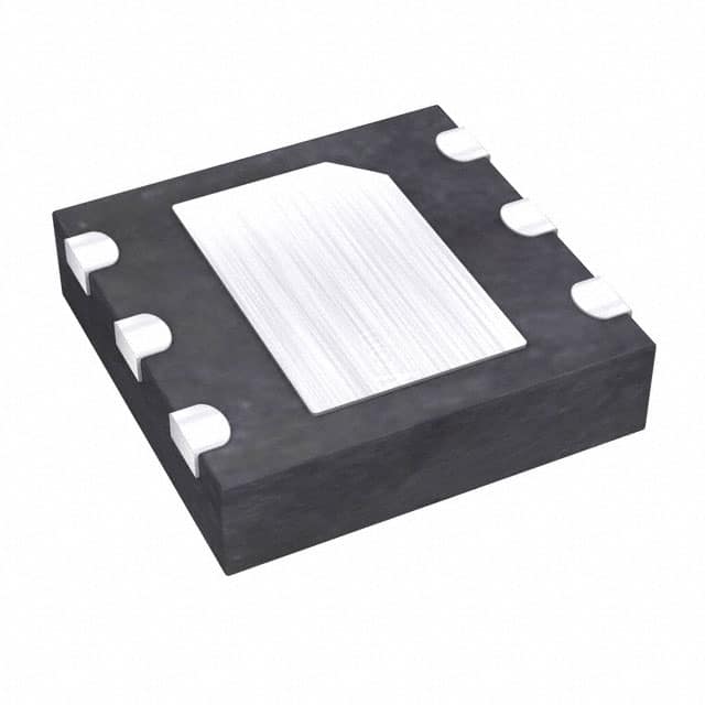
- Part No.:
- DS24B33Q+U
- Manufacturer:
- Analog Devices Inc./Maxim Integrated
- Category:
- Memory
- Package:
- 6-WDFN Exposed Pad
- Datasheet:
-
 DS24B33Q+U.pdf
- Description:
- IC EEPROM 4KBIT 1-WIRE 6TDFN
- Quantity:
- Payment:

- Shipping:

Inventory:1,547
Please send an inquiry. Send us your inquiry, and we will respond immediately.
Product details
Overview
DS24B33Q+U from Analog Devices is a 4096-bit, 1-Wire® EEPROM organized as 16 pages of 256 bits each, featuring a 32-byte scratchpad for verified write operations, unique 64-bit factory-programmed registration number, and open-drain IO interface operating from +2.8V to +5.25V at -40°C to +85°C. It serves as a secure, low-pin-count nonvolatile memory for calibration storage and board identification in parasitically powered sensor nodes.
For engineers reviewing the DS24B33Q+U datasheet, DS24B33Q+U pinout, DS24B33Q+U application, or DS24B33Q+U equivalent, this page delivers verified electrical specs (e.g., 15.4kbps/125kbps 1-Wire speeds, ±8kV contact ESD), package-specific terminal mapping (TDFN-EP, 6-pin), endurance (50k cycles @ +85°C), data retention (40 years @ +85°C), and functional compatibility with DS2433.
Technical Context
The DS24B33Q+U implements a parasitic-power 1-Wire slave architecture with strict timing compliance for standard (65µs slot) and overdrive (8µs slot) modes. Its IO pin functions as an open-drain bidirectional bus interface requiring external pullup, with hysteresis (0.2–1.7V) and switching thresholds (VTL = 0.5V, VTH = VPUP − 1.0V) optimized for noise immunity on shared buses.
Memory access follows a two-phase protocol: data is first written to the volatile 32-byte scratchpad and verified via CRC-16 before copying to EEPROM. The device uses three address registers (TA1, TA2, E/S) and supports ROM function commands (Match ROM, Search ROM) and memory commands (Write Scratchpad [0Fh], Copy Scratchpad [55h], Read Memory [F0h]) with LSB-first bit ordering.
Key Specifications
| Parameter | Value and Actual Design Meaning |
|---|---|
| Memory Capacity | 4096 bits (16 × 256-bit pages); enables storage of calibration constants, PCB IDs, and revision logs across multiple devices on one bus. |
| 1-Wire Speed | 15.4kbps standard / 125kbps overdrive; supports high-throughput configuration updates without dedicated clock lines. |
| Operating Voltage | +2.8V to +5.25V; compatible with common microcontroller I/O rails and parasitic power schemes. |
| Endurance | 50,000 write/erase cycles at +85°C; sufficient for field recalibration and firmware update logging in industrial environments. |
| Data Retention | 40 years at +85°C; ensures long-term integrity of calibration data in unattended equipment. |
| ESD Rating | ±8kV contact discharge (IEC 1000-4-2 Level 4); protects against handling damage during board assembly and field service. |
| IO Pin Type | Open-drain with 20mA sink capability; requires external pullup but eliminates need for level shifters in mixed-voltage systems. |
Pinout & Package
DS24B33Q+U is housed in a 6-pin TDFN-EP (3mm × 3mm) package with exposed pad soldered to ground plane for thermal and electrical stability. Pin 1 is N.C., Pin 2 is IO (1-Wire bus interface), Pin 3 is GND, Pins 4–6 are N.C., and the EP pad must be connected to system ground.
| Pin/Terminal | Circuit Role | Design Meaning |
|---|---|---|
| Pin 1 | Not Connected | No internal connection; must remain floating or tied to ground per layout best practice. |
| Pin 2 | IO | Open-drain 1-Wire bus interface; requires external pullup resistor (0.3–2.2kΩ) and handles bidirectional communication and power harvesting. |
| Pin 3 | GND | Ground reference for internal circuitry and parasitic power return path. |
| Pins 4–6 | Not Connected | No internal bond wires; may be left unconnected or used as thermal relief pads. |
| EP (Exposed Pad) | Thermal/Ground Plane | Mandatory solder connection to PCB ground plane for thermal dissipation and signal integrity; not electrically isolated. |
Key Features
| Feature | Design Value |
|---|---|
| 64-bit unique registration number | Factory-programmed serial ID with CRC-8 ensures absolute device identity and collision-free multidrop addressing on shared 1-Wire nets. |
| 256-bit scratchpad with verification | Volatile buffer allows full read-back and CRC-16 validation before committing to EEPROM, eliminating partial-write corruption in noisy environments. |
| Switchpoint hysteresis | 0.2–1.7V input hysteresis prevents false triggering from bus noise, enabling reliable operation in electrically harsh industrial settings. |
| Backward compatibility with DS2433 | Identical family code (0x23) and command set allow drop-in replacement in legacy designs without firmware changes. |
| Enhanced ESD protection | ±8kV contact discharge rating exceeds IEC 61000-4-2 Level 4, reducing field failure risk during handling and installation. |
Applications
| Calibration Data Storage | Board Identification |
|---|---|
Use Scenario: Storing temperature sensor offset coefficients, ADC gain trim values, and sensor linearity corrections during factory calibration. IC Role / Device Role / Timing Role: Nonvolatile memory slave on 1-Wire bus; provides tamper-resistant, low-pin-count storage accessible by host MCU during boot or maintenance mode. Use Value: Eliminates need for external SPI/I²C EEPROM and associated routing; enables per-unit calibration traceability using unique 64-bit ID. |
Use Scenario: Encoding PCB revision, manufacturing date, and serial number directly onto the board for automated test and field asset tracking. IC Role / Device Role / Timing Role: 1-Wire identity tag; responds to Search ROM commands to enumerate all boards on a single bus without address jumpers or DIP switches. Use Value: Reduces BOM count and assembly steps; supports zero-touch inventory management in distributed sensor networks. |
| Product Revision Logging | Firmware Configuration Storage |
Use Scenario: Recording software version, bootloader state, and hardware compatibility flags after field firmware updates. IC Role / Device Role / Timing Role: Write-once or infrequent-write EEPROM node; stores metadata critical for safe rollback and compatibility enforcement. Use Value: Prevents mismatched firmware/hardware combinations; enables deterministic recovery paths verified by host MCU at startup. |
Use Scenario: Holding user-configurable parameters (e.g., alarm thresholds, sampling intervals) that persist across power cycles. IC Role / Device Role / Timing Role: Low-power, parasitically powered configuration store; accessed only during setup or reconfiguration, minimizing bus contention. Use Value: Removes dependency on battery-backed RAM; supports fully passive, maintenance-free operation in remote monitoring nodes. |
Equivalent & Alternatives
The following parts are listed as comparable options for similar 1-Wire EEPROM applications.
| Alternative Part | Technical Difference | Application Difference | Selection Advice |
|---|---|---|---|
| DS2433+T&R | Same 4Kb capacity, TO-92/SO packages; no TDFN-EP option; lower ESD rating (±4kV contact). | Lacks exposed pad thermal performance; limited to through-hole or SOIC layouts. | Select DS2433+T&R only when legacy TO-92 footprint or cost-sensitive SOIC assembly is required. |
| DS24B33S+T&R | Identical core functionality; 8-pin SOIC package with pins 1,2,5–8 as N.C.; same TDFN-EP electrical specs but different mechanical form factor. | Requires PCB redesign for SOIC footprint; no exposed pad for thermal grounding. | Choose DS24B33S+T&R when board space allows SOIC and thermal demands are less stringent than TDFN-EP. |
Compared with DS24B33Q+U, DS2433+T&R offers lower-cost packaging but reduced ESD robustness and no thermal pad, while DS24B33S+T&R provides identical electrical behavior in SOIC format-making DS24B33Q+U the optimal choice for space-constrained, thermally demanding, or high-reliability 1-Wire node designs.
Availability
DS24B33Q+U is available at Aetrix Electronics and suitable for calibration data storage, board identification, and product revision logging requiring stable component supply across automotive Tier-1, industrial IoT, and medical device production programs.
Supply support for DS24B33Q+U includes scheduled delivery planning, volume procurement assistance, BOM continuity management, traceable sourcing, and lifecycle availability coordination for OEM customers, industrial embedded developers, connected-device designers, and electronics production programs.
Manufacturer
Analog Devices is a global semiconductor leader specializing in high-performance analog, mixed-signal, and digital signal processing technologies for precision measurement and connectivity applications.
The DS24B33Q+U belongs to Analog Devices' 1-Wire EEPROM product line, engineered for secure, low-pin-count, parasitically powered nonvolatile memory in distributed sensor and identification systems.
FAQ
What is the function of the exposed pad (EP) on the DS24B33Q+U?
The exposed pad on the DS24B33Q+U is a thermal and electrical ground connection that must be soldered evenly to the PCB's ground plane. It improves thermal dissipation during EEPROM programming (which draws 2mA) and enhances signal integrity on the 1-Wire bus by reducing noise coupling. Leaving the EP unconnected violates the device's operational specification and may cause intermittent communication or premature failure.
Is DS24B33Q+U pin-compatible with DS2433?
DS24B33Q+U is not pin-compatible with DS2433 due to its 6-pin TDFN-EP package versus DS2433's 2-pin TO-92 or 8-pin SOIC variants. While both share identical 1-Wire command sets and memory architecture, the DS24B33Q+U requires a custom footprint with EP grounding. Software and protocol-level compatibility is maintained, but PCB layout changes are mandatory for substitution.
How does the scratchpad verification process work in DS24B33Q+U?
In DS24B33Q+U, data is first written to the 32-byte scratchpad using the Write Scratchpad [0Fh] command. The device calculates a CRC-16 of the command, target address, and data bytes. The host can then read back the scratchpad contents-including TA1, TA2, and E/S register-and verify integrity before issuing Copy Scratchpad [55h]. If the PF (partial byte) flag is set or AA (authorization accepted) remains unset, the write failed and must be retried.
What is the maximum number of DS24B33Q+U devices supported on a single 1-Wire bus?
The DS24B33Q+U supports multidrop operation with no hard upper limit on device count-only constrained by bus capacitance, pullup strength, and timing margins. In practice, up to 100 devices have been validated on properly terminated 1-Wire buses using active pullups like the DS2482-100. Each DS24B33Q+U is uniquely addressed via its factory-programmed 64-bit ROM ID, enabling individual access without address conflicts.
Does DS24B33Q+U require an external power supply (VCC) or operate parasitically?
DS24B33Q+U operates exclusively in parasitic power mode-it derives all operating energy from the 1-Wire bus via the IO pin and requires no separate VCC connection. During EEPROM programming, the IO line must maintain ≥2.8V under load; therefore, the external pullup must be sized to sustain voltage during the 5ms tPROG interval, especially in multi-device networks where bus capacitance increases current demand.
DS24B33Q+U Specifications
- Product attributes
- Attribute value
- Manufacturer:
- Analog Devices Inc./Maxim Integrated
- Series:
- -
- Package/Case:
- 6-WDFN Exposed Pad
- Packaging:
- Bulk
- Product Status:
- Active
- Programmable:
- Not Verified
- Memory Type:
- Non-Volatile
- Memory Format:
- EEPROM
- Technology:
- EEPROM
- Memory Size:
- 4Kbit
- Memory Organization:
- 256 x 16
- Memory Interface:
- 1-Wire®
- Clock Frequency:
- -
- Write Cycle Time - Word, Page:
- -
- Access Time:
- 2 µs
- Voltage - Supply:
- 2.8V ~ 5.25V
- Operating Temperature:
- -40°C ~ 85°C (TA)
- Grade:
- -
- Qualification:
- -
- Mounting Type:
- Surface Mount
- Supplier Device Package:
- 6-TDFN (3x3)
DS24B33Q+U FAQ
1.How can I place an order for DS24B33Q+U through Aetrix?
Please submit a Request for Quotation (RFQ) for DS24B33Q+U on Aetrix. Our sales agent will provide a competitive quotation and guide you through the order confirmation once you accept the terms.
2.Are the price and stock information for DS24B33Q+U reliable?
The price and inventory of DS24B33Q+U are updated periodically and may fluctuate due to market conditions. Stock and pricing data are typically refreshed every 24 hours. Quotation validity for DS24B33Q+U is usually 5 days.
3.What payment methods are accepted for DS24B33Q+U?
We accept Wire Transfer, PayPal, Credit Card, Western Union, MoneyGram, and Escrow for DS24B33Q+U transactions.
Note: Certain payment methods may incur a processing fee.
4.How is shipping managed for DS24B33Q+U?
DS24B33Q+U orders can be shipped via leading logistics carriers, including DHL, UPS, FedEx, TNT, or Registered Mail.
Once your DS24B33Q+U order is processed, you will receive an email with the shipment details and tracking number.
Note: Tracking information may take up to 24 hours to appear. Express delivery typically takes 3–5 business days.
5.How can I obtain technical support or documentation for DS24B33Q+U?
For technical support, including DS24B33Q+U datasheets, pinout diagrams, or application guidance, please contact our engineering support team. They can provide detailed documentation and assistance for your DS24B33Q+U requirements.
6.How does Aetrix verify that DS24B33Q+U is sourced from the original manufacturer or authorized distributors?
All DS24B33Q+U products on Aetrix are procured from qualified distributors and authorized channels. Our dedicated quality assurance team conducts strict verification, including traceability checks and, if necessary, third-party testing. This ensures that DS24B33Q+U meets industry standards.
7.What is the process for return or replacement of DS24B33Q+U?
All DS24B33Q+U units undergo pre-shipment inspection (PSI). If there is an issue with DS24B33Q+U, returns or replacements are accepted under the following conditions:
1.Quantity discrepancies, incorrect items, or visible external defects (such as breakage or corrosion), acknowledged by Aetrix.
2.The issue is reported within 90 days of delivery.
3.The DS24B33Q+U part is unused and in its original packaging.
Return procedure for DS24B33Q+U:
1.Submit a request within 90 days.
2.Obtain a Return Material Authorization (RMA) from Aetrix.
DS24B33Q+U Tags

-
M24C02-WMN6TP
STMicroelectronics

-
AT24C02C-XHM-T
Microchip Technology

-
AT21CS01-STUM10-T
Microchip Technology

-
AT24C02C-SSHM-T
Microchip Technology

-
24LC01BT-I/OT
Microchip Technology

-
M24C02-FMC6TG
STMicroelectronics
-
AT24CS02-SSHM-T
Microchip Technology

-
93LC46BT-I/OT
Microchip Technology
-
AT24C04C-SSHM-T
Microchip Technology

-
24LC01BT-I/SN
Microchip Technology
-
24AA02UIDT-I/OT
Microchip Technology

-
AT24C08C-STUM-T
Microchip Technology
Tech Hub

Schmitt triggers use separate rising and falling thresholds to stabilize slow or noisy signals. This guide covers hysteresis, 74HC14 and 74HCT14 selection, comparator calculations, RC oscillators and p…

Counterfeit components can hide behind convincing markings and passing basic function tests. This engineering reference covers source traceability, external inspection, X-ray, XRF, electrical testing, …

A practical engineering and sourcing framework covering lifecycle verification, lifetime-buy calculations, replacement qualification, supplier checks and counterfeit-risk controls.

TTL and CMOS logic families differ in thresholds, loading, output drive, power and timing. This engineering guide compares 74HC and 74HCT, calculates noise margins and checks 3.3 V/5 V compatibility.

A practical engineering guide to 3.3V and 5V logic compatibility, input thresholds, resistor dividers, translator ICs, MOSFET level shifting, I2C pull-ups, timing limits and power-sequencing risks.

The 74HC595 uses push-pull logic outputs, while the TPIC6B595 uses 50 V open-drain DMOS sinks for higher-power loads. This guide compares timing, current limits, 3.3 V interfacing, load wiring, thermal…

The 74HC595 converts serial data into eight stable parallel outputs. This guide covers pin functions, shift and storage timing, OE and MR behavior, drive-current limits, cascading, voltage compatibilit…

A technical comparison of level-sensitive latches and edge-triggered flip-flops, covering timing windows, setup and hold limits, master–slave operation, time borrowing, race-through, HDL inference and…

A D latch stores one bit while Enable controls when data can pass. This reference covers gate-level operation, truth tables, transparency, setup and hold timing, LE versus OE, common ICs and practical …

An SR latch stores one bit through cross-coupled feedback. This engineering reference covers NOR and NAND implementations, truth tables, forbidden-state recovery, gated operation, switch debouncing, fa…


