
 My Inquiry
 My Account


Analog Devices Inc./Maxim Integrated DS2502X1+
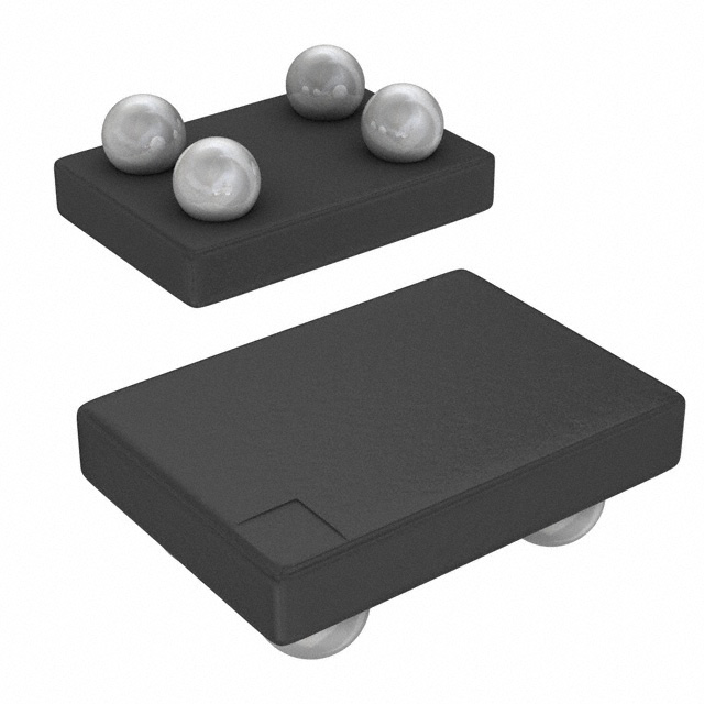
- Part No.:
- DS2502X1+
- Manufacturer:
- Analog Devices Inc./Maxim Integrated
- Category:
- Memory
- Package:
- 4-UFBGA, WLCSP
- Datasheet:
-
 DS2502X1+.pdf
- Description:
- IC EPROM 1KBIT 1-WIRE 4WLP
- Quantity:
- Payment:

- Shipping:

Inventory:1,599
Please send an inquiry. Send us your inquiry, and we will respond immediately.
Product details
Overview
DS2502X1+ from Maxim Integrated is a 1-Wire add-only memory IC with factory-lasered 64-bit ROM ID, 1024-bit EPROM (4 × 256-bit pages), page-level write protection, and parasitic power operation - used for asset traceability, calibration storage, and maintenance logging in industrial sensors and medical devices.
For engineers reviewing the DS2502X1+ datasheet, DS2502X1+ pinout, DS2502X1+ application, or DS2502X1+ equivalent, this device supports single-pin 1-Wire communication at up to 16.3 kbps, operates from 2.8V–6.0V (−40°C to +85°C), requires 11.5–12.0V for programming, and delivers guaranteed unique identification via laser-programmed 48-bit serial number + 8-bit CRC + 8-bit family code (09h).
Technical Context
The DS2502X1+ implements a hierarchical 1-Wire protocol: ROM function commands (Read/Match/Search/Skip ROM) must precede memory access, enabling multi-drop network addressing. Its internal architecture includes a 8-bit scratchpad buffer, on-chip 8-bit CRC generator, and parasitic power harvesting circuitry that stores charge during high bus states to sustain operation during low states.
EPROM programming follows bit-wise 1→0 transitions only; data integrity is enforced via command/address/data CRC verification before each 480 µs 12V programming pulse. Page address redirection bytes (in status memory) allow software-level patching by invalidating old pages and mapping to new ones - no hardware erase required.
Key Specifications
| Parameter | Value and Actual Design Meaning |
|---|---|
| Memory Type | 1024-bit EPROM (4 pages × 256 bits), plus 64-bit lasered ROM and 64-bit status memory |
| Interface | Single-pin 1-Wire (open-drain), bidirectional, parasitic-power capable |
| Operating Voltage | 2.8V–6.0V for read; 11.5V–12.0V for programming (−40°C to +50°C) |
| Temperature Range | −40°C to +85°C (industrial grade) |
| Data Rate | Up to 16.3 kbps standard speed; supports overdrive mode |
| Unique ID | Factory-lasered 64-bit ROM: 8-bit family code (09h) + 48-bit serial number + 8-bit CRC |
| Write Protection | Per-page permanent write lock via status byte bits; irreversible once set |
Pinout & Package
DS2502X1+ uses a 4-terminal Wafer-Level Package (WLP), qualified for electro-mechanical contact applications. No soldering permitted. Laser-marked top side shows revision/date; contacts are not visible in standard top view.
| Pin/Terminal | Circuit Role | Design Meaning |
|---|---|---|
| 1A / 1B | DATA (1-Wire I/O) | Open-drain bidirectional signal line; carries power, clock, address, and data via time-division multiplexing |
| 2A / 2B | GND | Ground reference for parasitic power return path and logic reference |
Key Features
| Feature | Design Value |
|---|---|
| Add-only memory architecture | Enables field-updatable calibration or revision data without erasing prior content - critical for tamper-resistant firmware logs |
| Page address redirection | Allows software to logically replace outdated EPROM pages by redirecting reads to newly programmed pages - eliminates need for external memory management |
| Factory-lasered 64-bit ROM ID | Provides cryptographically verifiable, collision-free device identity for secure asset tracking and anti-counterfeiting systems |
| Parasitic power operation | Eliminates dedicated VCC pin and bypass capacitor - reduces BOM count and PCB footprint in space-constrained sensor nodes |
| Per-page write protection | Locks individual 256-bit pages permanently after programming - prevents accidental or malicious overwrite of critical calibration constants |
Applications
| Industrial Sensor Calibration | Medical Device Asset Tracking |
|---|---|
|
Use Scenario: Storing temperature compensation coefficients and sensor offset values during factory calibration of pressure transducers. IC Role / Device Role / Timing Role: Nonvolatile memory node providing immutable, traceable calibration data accessible via microcontroller's GPIO pin. Use Value: Eliminates need for external EEPROM or battery-backed RAM; enables post-deployment recalibration verification using the guaranteed-unique 48-bit serial number. |
Use Scenario: Embedding sterilization cycle history and usage counters into reusable surgical instruments. IC Role / Device Role / Timing Role: Tamper-evident identity and log storage element interfaced directly to handheld reader via 1-Wire contact probe. Use Value: Supports HIPAA-compliant audit trails with cryptographic traceability - each instrument's DS2502X1+ ID links to centralized database records. |
| Smart Meter Firmware Revision | Automotive Aftermarket Module Authentication |
|
Use Scenario: Recording firmware version, patch level, and update timestamps inside utility smart meters deployed in harsh outdoor environments. IC Role / Device Role / Timing Role: Read-only configuration memory accessed during boot sequence to validate firmware integrity and enable feature gating. Use Value: Prevents rollback attacks via write-protected status bytes; allows field updates while preserving historical revision metadata across power cycles. |
Use Scenario: Authenticating OEM-approved replacement modules (e.g., cabin air filters, brake pads) using embedded DS2502X1+ identifiers. IC Role / Device Role / Timing Role: Secure identity anchor verifying module origin and compatibility before enabling vehicle CAN bus integration. Use Value: Leverages factory-lasered ROM ID and CRC to block counterfeit parts - no cryptographic engine required on host ECU. |
Equivalent & Alternatives
The following parts are listed as comparable options for similar add-only memory applications.
| Alternative Part | Technical Difference | Application Difference | Selection Advice |
|---|---|---|---|
| DS2430A+ | 256-bit EEPROM (not EPROM); supports full read/write cycles; no page redirection; 4-pin TSOC/WLP | Lacks permanent write protection and page patching; suitable for dynamic parameter storage but not for immutable traceability | Choose DS2430A+ only if field rewrites are required and cryptographic traceability is not needed. |
| DS28EC20 | 20kb 1-Wire EEPROM; integrated SHA-256 authentication; 4-pin TDFN/WLP; 1.7–5.25V operation | Includes hardware crypto engine and flexible memory partitioning; higher cost and complexity than DS2502X1+ | Select DS28EC20 when FIPS-compliant authentication or frequent secure writes are mandatory - not for simple add-only use cases. |
Compared with DS2502X1+, DS2430A+ offers rewritable memory but sacrifices guaranteed uniqueness and page-level immutability, while DS28EC20 adds cryptographic security at the expense of power efficiency and design simplicity - DS2502X1+ remains optimal for cost-sensitive, tamper-proof traceability where data is written once and verified many times.
Availability
DS2502X1+ is available at Aetrix Electronics and suitable for industrial sensor calibration, medical device asset tracking, and smart meter firmware revision management requiring stable component supply and long-term lifecycle support.
Supply support for DS2502X1+ includes scheduled delivery planning, volume procurement assistance, BOM continuity management, traceable sourcing, and lifecycle availability coordination for OEM customers, industrial embedded developers, connected-device designers, and electronics production programs.
Manufacturer
Maxim Integrated (now part of Analog Devices) designs precision analog, mixed-signal, and digital ICs for industrial, automotive, and communications applications.
The DS2502X1+ belongs to Maxim's 1-Wire memory product line, engineered specifically for low-pin-count, parasitic-powered identification and immutable data logging in resource-constrained embedded systems.
FAQ
What is the primary function of the DS2502X1+ in an embedded system?
The DS2502X1+ serves as a tamper-resistant, single-pin 1-Wire add-only memory IC that stores immutable calibration data, asset IDs, and maintenance logs. Its factory-lasered 64-bit ROM provides guaranteed unique identification, while its 1024-bit EPROM supports page-level write protection and software-driven page redirection - making DS2502X1+ ideal for traceability-critical applications where data must be appended but never altered or erased.
Does the DS2502X1+ require an external power supply?
No, the DS2502X1+ operates entirely on parasitic power harvested from the 1-Wire data line during high-voltage periods, eliminating the need for a dedicated VCC pin or bypass capacitor. During read operations (2.8V–6.0V), it sustains functionality using internal capacitance; programming requires a separate 11.5–12.0V pulse applied to the same DATA line - confirming DS2502X1+'s true single-wire, zero-external-power architecture.
How does the DS2502X1+ ensure data integrity during programming?
The DS2502X1+ enforces data integrity through mandatory 8-bit CRC verification before every programming pulse: the bus master computes CRC over command, address, and data bytes; DS2502X1+ returns its own CRC for comparison. Only upon match does the 480 µs 12V pulse initiate bit-wise 1→0 programming. Post-pulse, the master reads back the target byte to confirm correct bit state - ensuring DS2502X1+ writes are both validated and verifiable.
Can the DS2502X1+ be used in multi-drop 1-Wire networks?
Yes, the DS2502X1+ includes a built-in multidrop controller compliant with the standard 1-Wire bus specification. Its 64-bit ROM ID enables unambiguous device enumeration via Search ROM commands, allowing dozens of DS2502X1+ units (and other 1-Wire devices) to coexist on a single data line - all addressed individually without contention, making DS2502X1+ suitable for distributed sensor arrays and modular equipment identification systems.
What package type does the DS2502X1+ use, and what are its assembly requirements?
The DS2502X1+ is supplied in a 4-terminal Wafer-Level Package (WLP), optimized for electro-mechanical contact interfaces - not solder reflow. Assembly requires spring-loaded pogo pins or compliant contact probes aligned to the laser-marked top surface; soldering voids qualification and risks damage. This WLP form factor enables ultra-compact integration into wearable sensors and disposable medical cartridges where DS2502X1+'s minimal footprint and contact-based interface deliver mechanical and electrical reliability.
DS2502X1+ Specifications
- Product attributes
- Attribute value
- Manufacturer:
- Analog Devices Inc./Maxim Integrated
- Series:
- -
- Package/Case:
- 4-UFBGA, WLCSP
- Packaging:
- Tape & Reel (TR)
- Product Status:
- Active
- Programmable:
- Not Verified
- Memory Type:
- Non-Volatile
- Memory Format:
- EPROM
- Technology:
- EPROM - OTP
- Memory Size:
- 1Kbit
- Memory Organization:
- 128 x 8
- Memory Interface:
- 1-Wire®
- Clock Frequency:
- -
- Write Cycle Time - Word, Page:
- -
- Access Time:
- -
- Voltage - Supply:
- 2.8V ~ 6V
- Operating Temperature:
- -40°C ~ 85°C (TA)
- Grade:
- -
- Qualification:
- -
- Mounting Type:
- Surface Mount
- Supplier Device Package:
- 4-WLP (1.62x0.93)
DS2502X1+ FAQ
1.How can I place an order for DS2502X1+ through Aetrix?
Please submit a Request for Quotation (RFQ) for DS2502X1+ on Aetrix. Our sales agent will provide a competitive quotation and guide you through the order confirmation once you accept the terms.
2.Are the price and stock information for DS2502X1+ reliable?
The price and inventory of DS2502X1+ are updated periodically and may fluctuate due to market conditions. Stock and pricing data are typically refreshed every 24 hours. Quotation validity for DS2502X1+ is usually 5 days.
3.What payment methods are accepted for DS2502X1+?
We accept Wire Transfer, PayPal, Credit Card, Western Union, MoneyGram, and Escrow for DS2502X1+ transactions.
Note: Certain payment methods may incur a processing fee.
4.How is shipping managed for DS2502X1+?
DS2502X1+ orders can be shipped via leading logistics carriers, including DHL, UPS, FedEx, TNT, or Registered Mail.
Once your DS2502X1+ order is processed, you will receive an email with the shipment details and tracking number.
Note: Tracking information may take up to 24 hours to appear. Express delivery typically takes 3–5 business days.
5.How can I obtain technical support or documentation for DS2502X1+?
For technical support, including DS2502X1+ datasheets, pinout diagrams, or application guidance, please contact our engineering support team. They can provide detailed documentation and assistance for your DS2502X1+ requirements.
6.How does Aetrix verify that DS2502X1+ is sourced from the original manufacturer or authorized distributors?
All DS2502X1+ products on Aetrix are procured from qualified distributors and authorized channels. Our dedicated quality assurance team conducts strict verification, including traceability checks and, if necessary, third-party testing. This ensures that DS2502X1+ meets industry standards.
7.What is the process for return or replacement of DS2502X1+?
All DS2502X1+ units undergo pre-shipment inspection (PSI). If there is an issue with DS2502X1+, returns or replacements are accepted under the following conditions:
1.Quantity discrepancies, incorrect items, or visible external defects (such as breakage or corrosion), acknowledged by Aetrix.
2.The issue is reported within 90 days of delivery.
3.The DS2502X1+ part is unused and in its original packaging.
Return procedure for DS2502X1+:
1.Submit a request within 90 days.
2.Obtain a Return Material Authorization (RMA) from Aetrix.
DS2502X1+ Tags

-
M24C02-WMN6TP
STMicroelectronics

-
AT24C02C-XHM-T
Microchip Technology

-
AT21CS01-STUM10-T
Microchip Technology

-
AT24C02C-SSHM-T
Microchip Technology

-
24LC01BT-I/OT
Microchip Technology

-
M24C02-FMC6TG
STMicroelectronics
-
AT24CS02-SSHM-T
Microchip Technology

-
93LC46BT-I/OT
Microchip Technology
-
AT24C04C-SSHM-T
Microchip Technology

-
24LC01BT-I/SN
Microchip Technology
-
24AA02UIDT-I/OT
Microchip Technology

-
AT24C08C-STUM-T
Microchip Technology
Tech Hub

A practical engineering guide to 3.3V and 5V logic compatibility, input thresholds, resistor dividers, translator ICs, MOSFET level shifting, I2C pull-ups, timing limits and power-sequencing risks.

The 74HC595 uses push-pull logic outputs, while the TPIC6B595 uses 50 V open-drain DMOS sinks for higher-power loads. This guide compares timing, current limits, 3.3 V interfacing, load wiring, thermal…

The 74HC595 converts serial data into eight stable parallel outputs. This guide covers pin functions, shift and storage timing, OE and MR behavior, drive-current limits, cascading, voltage compatibilit…

A technical comparison of level-sensitive latches and edge-triggered flip-flops, covering timing windows, setup and hold limits, master–slave operation, time borrowing, race-through, HDL inference and…

A D latch stores one bit while Enable controls when data can pass. This reference covers gate-level operation, truth tables, transparency, setup and hold timing, LE versus OE, common ICs and practical …

An SR latch stores one bit through cross-coupled feedback. This engineering reference covers NOR and NAND implementations, truth tables, forbidden-state recovery, gated operation, switch debouncing, fa…

Latch circuits retain one bit through feedback. This technical reference covers SR and D latches, truth tables, transparency, timing limits, latch-versus-flip-flop behavior, applications and common log…

An engineering guide to LED driver operation, constant-current and constant-voltage outputs, linear and switching topologies, dimming, IC selection, calculations, replacement compatibility, and fault c…

Operational amplifier guide covering op amp basics, feedback, ideal vs real op amps, common configurations, buffer circuits, offset, bias current, gain-bandwidth, slew rate, rail-to-rail limits and sel…

Jumper cables guide covering safe connection order, red and black clamp placement, final ground connection, cable gauge, length, clamp quality, copper vs CCA cables, jump starter comparison and battery…


