
 My Inquiry
 My Account


Texas Instruments DS250DF810ABVT
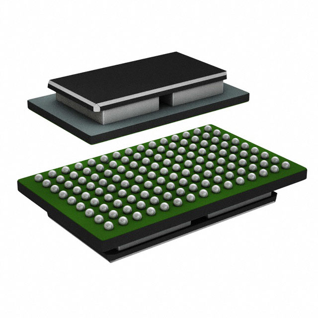
- Part No.:
- DS250DF810ABVT
- Manufacturer:
- Texas Instruments
- Category:
- Specialized
- Package:
- 135-BGA Module
- Datasheet:
-
 DS250DF810ABVT.pdf
- Description:
- IC INTFACE SPECIALIZED 135FCBGA
- Quantity:
- Payment:

- Shipping:

Inventory:227
Please send an inquiry. Send us your inquiry, and we will respond immediately.
Product details
Overview
DS250DF810ABVT from Texas Instruments is an octal-channel multi-rate retimer IC designed for 20.2752–25.8 Gbps serial data links, featuring integrated adaptive CTLE/DFE equalization, low-jitter 3-tap FIR transmit filtering, on-chip AC coupling capacitors, and 2×2 cross-point switching per channel pair. It enables IEEE 802.3bj 100GbE, InfiniBand EDR, and OIF-CEI-25G-LR/MR/SR/VSR compliance in high-loss backplane and optical front-port applications.
For engineers reviewing the DS250DF810ABVT datasheet, DS250DF810ABVT pinout, DS250DF810ABVT application, or DS250DF810ABVT equivalent, this page delivers verified technical context, validated pin functions, confirmed power and signal integrity specs (2.5 V supply, 135-pin fcBGA, 8 mm × 13 mm), and real-world retiming use cases - all extracted from TI's production-grade SNLS513C datasheet (Rev C, Oct 2019).
Technical Context
The DS250DF810ABVT implements independent per-channel CDR with adaptive continuous-time linear equalization (CTLE) and decision feedback equalization (DFE), supporting full-rate (20.2752–25.8 Gbps), half-rate (10.1376–12.9 Gbps), and quarter-rate (5.0688–6.45 Gbps) operation. Its integrated 2×2 cross-point per lane pair enables lane swapping and fanout without external routing.
It operates from a single 2.5 V ±5% supply, requires no external reference clock, and embeds physical 220 nF AC coupling capacitors on all eight RX/TX differential pairs - eliminating 16 discrete capacitors and reducing PCB routing complexity. Calibration uses a 25 MHz ±100 ppm CMOS clock (CAL_CLK_IN) for VCO range tuning, not data recovery.
Key Specifications
| Parameter | Value and Actual Design Meaning |
|---|---|
| Data Rate Range | 20.2752–25.8 Gbps full-rate; supports sub-rates including 10.3125 Gbps and 12.5 Gbps for FEC pass-through |
| Supply Voltage | 2.5 V ±5%; six decoupling caps required (four 0.1 µF + two 1 µF) placed near VDD pins |
| Latency | <500 ps typical at 25.78125 Gbps - critical for low-latency interconnects like HPC and AI fabric |
| Transmit Amplitude | Adjustable 205–1225 mVppd (typical); resolution <50 mVppd between adjacent c(0) settings |
| Channel Loss Compensation | Supports ≥35 dB loss at 12.9 GHz via combined CTLE+DFE+FIR equalization |
| Package | 135-pin flip-chip BGA (fcBGA), 0.8 mm pitch, 8.0 mm × 13.0 mm body size |
| Input Sensitivity | VSDAT = 196 mVppd (ON threshold), VSDDT = 147 mVppd (OFF threshold) at 25.78125 Gbps, PRBS7, 20 dB loss |
Pinout & Package
DS250DF810ABVT is housed in a 135-pin flip-chip ball grid array (fcBGA) package with 0.8 mm pitch and 8.0 mm × 13.0 mm footprint. The pinout supports flow-through routing with high-speed differential I/Os arranged to allow signal traces beneath the package, minimizing stub length and impedance discontinuity.
| Pin/Terminal | Circuit Role | Design Meaning |
|---|---|---|
| RX0P / RX0N – RX7P / RX7N | Differential inputs | AC-coupled (220 nF on-chip), 100 Ω internal termination; support 20.2752–25.8 Gbps with adaptive CTLE/DFE |
| TX0P / TX0N – TX7P / TX7N | Differential outputs | 50 Ω drivers with on-chip 220 nF AC coupling; 3-tap FIR filter, adjustable amplitude (205–1225 mVppd) |
| CAL_CLK_IN / CAL_CLK_OUT | Calibration clock interface | 25 MHz ±100 ppm CMOS input (E1); buffered 2.5 V output (E15) for daisy-chaining multiple devices |
| ADDR0 / ADDR1 / EN_SMB | SMBus address & mode control | 4-level strap pins (GND/10kΩ/float/VDD) enabling 16 unique SMBus addresses and master/slave selection |
| SDA / SDC / READ_EN_N / ALL_DONE_N / INT_N | SMBus & status signaling | 3.3 V LVCMOS-tolerant open-drain I/Os; external 2–5 kΩ pull-ups required; INT_N supports wired-OR interrupt aggregation |
| VDD / GND | Power distribution | 13 dedicated VDD pins (2.5 V ±5%) and 102 GND balls ensure low-impedance return paths for high-speed signaling |
Key Features
| Feature | Design Value |
|---|---|
| Integrated AC coupling | Physical 220 nF capacitors on all 16 high-speed lanes eliminate 16 external components and reduce board area |
| Per-channel adaptive equalization | Independent CTLE + DFE per lane enables robust link training across heterogeneous channel losses |
| On-chip eye opening monitor (EOM) | Real-time in-system diagnostics without external test equipment; supports PRBS7/9 generator/checker |
| 2×2 cross-point per channel pair | Enables lane crossing and fanout within same device - avoids external mux or FPGA logic for topology flexibility |
| Single-supply operation | No low-jitter reference clock required; simplifies system clock tree and reduces BOM cost and layout complexity |
Applications
| Backplane Reach Extension | Jitter Cleaning for Optical Front-Ports |
|---|---|
Use Scenario: Extending 100GbE signals over >1m FR4 backplanes with multiple connectors and crosstalk-induced ISI. IC Role / Device Role / Timing Role: Retimer with per-lane CDR and adaptive equalization restores signal integrity and resets jitter budget. Use Value: Enables reliable 25.78125 Gbps operation across lossy channels with ≥35 dB insertion loss at 12.9 GHz. |
Use Scenario: Reconditioning high-speed serial data from QSFP28/CFP4 optical modules before host ASIC ingestion. IC Role / Device Role / Timing Role: Jitter cleaner and signal conditioner that recovers clean clocks and data from degraded optical receiver outputs. Use Value: Achieves BER ≤10⁻¹⁵ while compensating for transmitter jitter accumulation and fiber dispersion effects. |
| IEEE 802.3bj 100GbE Compliance | InfiniBand EDR Electrical Interface |
Use Scenario: Implementing KR4/KR2 electrical interfaces in switch line cards requiring forward error correction (FEC) pass-through. IC Role / Device Role / Timing Role: Multi-rate retimer supporting independent lane locking at 25.78125 Gbps and sub-rates (e.g., 12.5 Gbps) for FEC alignment. Use Value: Maintains lane-to-lane skew tolerance while enabling individual lane FEC transparency without protocol awareness. |
Use Scenario: Interfacing EDR-capable host adapters and target devices across mid-plane interconnects with >25 dB loss. IC Role / Device Role / Timing Role: Signal conditioning retimer with adaptive DFE and low-latency (<500 ps) re-timing for deterministic latency-sensitive fabrics. Use Value: Delivers sub-1 ns deterministic latency and supports EDR's 25.78125 Gbps per lane with full backward compatibility to FDR/QDR. |
Equivalent & Alternatives
The following parts are listed as comparable options for similar retimer applications.
| Alternative Part | Technical Difference | Application Difference | Selection Advice |
|---|---|---|---|
| DS250DF210ABVT | Quad-channel version (vs. octal); identical architecture, same 20.2752–25.8 Gbps range and equalization features | Used where only four lanes require retiming - lower power (≈50% of DS250DF810ABVT active-mode draw) and smaller PCB footprint | Select DS250DF210ABVT when lane count is ≤4 and board space/power budget is constrained. |
| DS125DF410ABVT | Quad-channel, supports up to 12.5 Gbps (vs. 25.8 Gbps); lacks DFE, uses fixed CTLE and 2-tap FIR | Targeted at 10GbE/25GbE SR/LR and PCIe Gen3/Gen4 - insufficient for 100GbE KR4 or InfiniBand EDR | Choose DS125DF410ABVT only for legacy 12.5 Gbps systems where cost and simplicity outweigh bandwidth needs. |
Compared with DS250DF210ABVT and DS125DF410ABVT, the DS250DF810ABVT uniquely delivers octal-channel 25+ Gbps retiming with adaptive DFE and on-chip AC coupling - making it the sole option for new 100GbE backplane and EDR fabric designs requiring full-lane-count, high-fidelity signal restoration.
Availability
DS250DF810ABVT is available at Aetrix Electronics and suitable for high-speed interconnect design, optical module integration, and 100GbE/EDR infrastructure development requiring stable component supply and long-term lifecycle assurance.
Supply support for DS250DF810ABVT includes scheduled delivery planning, volume procurement assistance, BOM continuity management, traceable sourcing, and lifecycle availability coordination for OEM customers, industrial embedded developers, connected-device designers, and electronics production programs.
Manufacturer
Texas Instruments is a global semiconductor leader specializing in analog, embedded processing, and high-speed interface solutions, with decades of expertise in signal integrity and retimer technology.
The DS250DF810ABVT belongs to TI's DS250DF family of multi-rate retimers, engineered specifically for next-generation data center and HPC interconnects demanding 25+ Gbps per lane, ultra-low latency, and adaptive equalization in compact BGA packages.
FAQ
What is the maximum supported data rate for DS250DF810ABVT?
The DS250DF810ABVT supports a continuous full-rate range of 20.2752 Gbps to 25.8 Gbps, including key sub-rates such as 10.3125 Gbps and 12.5 Gbps for Forward Error Correction pass-through. At 25.78125 Gbps (100GbE KR4), it achieves <500 ps typical latency and supports ≥35 dB channel loss at 12.9 GHz via combined CTLE, DFE, and 3-tap FIR equalization - all verified in TI's SNLS513C datasheet.
Does DS250DF810ABVT require an external reference clock?
No, the DS250DF810ABVT does not require an external low-jitter reference clock for data recovery. It uses an internal CDR architecture. A 25 MHz ±100 ppm CMOS calibration clock (CAL_CLK_IN) is required solely for VCO frequency range calibration - not for timing recovery - and may be shared across multiple devices via CAL_CLK_OUT daisy-chaining.
How many power supply pins does DS250DF810ABVT have, and what voltage is required?
The DS250DF810ABVT has 13 dedicated VDD pins and requires a single 2.5 V ±5% supply (2.375–2.625 V). TI mandates placement of at least six decoupling capacitors - four 0.1 µF and two 1 µF - directly beneath or adjacent to the device to maintain supply noise below 10 mVpp above 10 MHz, as specified in Section 8.3 of the SNLS513C datasheet.
Can DS250DF810ABVT operate in both SMBus master and slave modes?
Yes, DS250DF810ABVT supports dual SMBus modes. SMBus slave mode is enabled by pulling EN_SMB to VDD (1 kΩ), allowing register access via standard I²C commands. SMBus master mode is activated by floating EN_SMB, enabling autonomous EEPROM configuration loading - with READ_EN_N initiating reads and ALL_DONE_N signaling completion. Both modes use 3.3 V-tolerant SDA/SDC pins requiring external 2–5 kΩ pull-ups.
What package type and dimensions does DS250DF810ABVT use?
The DS250DF810ABVT uses a 135-pin flip-chip BGA (fcBGA) package with 0.8 mm ball pitch and nominal body dimensions of 8.0 mm × 13.0 mm. This compact, flow-through routing-optimized package places high-speed RX/TX pairs on opposite edges to enable signal traces underneath the device - minimizing stub length and preserving signal integrity at 25+ Gbps.
DS250DF810ABVT Specifications
- Product attributes
- Attribute value
- Manufacturer:
- Texas Instruments
- Series:
- -
- Package/Case:
- 135-BGA Module
- Packaging:
- Tape & Reel (TR)
- Product Status:
- Active
- Applications:
- Retimer
- Interface:
- -
- Voltage - Supply:
- -
- Supplier Device Package:
- 135-FCBGA (8.05x13.05)
- Grade:
- -
- Qualification:
- -
- Mounting Type:
- Surface Mount
DS250DF810ABVT FAQ
1.How can I place an order for DS250DF810ABVT through Aetrix?
Please submit a Request for Quotation (RFQ) for DS250DF810ABVT on Aetrix. Our sales agent will provide a competitive quotation and guide you through the order confirmation once you accept the terms.
2.Are the price and stock information for DS250DF810ABVT reliable?
The price and inventory of DS250DF810ABVT are updated periodically and may fluctuate due to market conditions. Stock and pricing data are typically refreshed every 24 hours. Quotation validity for DS250DF810ABVT is usually 5 days.
3.What payment methods are accepted for DS250DF810ABVT?
We accept Wire Transfer, PayPal, Credit Card, Western Union, MoneyGram, and Escrow for DS250DF810ABVT transactions.
Note: Certain payment methods may incur a processing fee.
4.How is shipping managed for DS250DF810ABVT?
DS250DF810ABVT orders can be shipped via leading logistics carriers, including DHL, UPS, FedEx, TNT, or Registered Mail.
Once your DS250DF810ABVT order is processed, you will receive an email with the shipment details and tracking number.
Note: Tracking information may take up to 24 hours to appear. Express delivery typically takes 3–5 business days.
5.How can I obtain technical support or documentation for DS250DF810ABVT?
For technical support, including DS250DF810ABVT datasheets, pinout diagrams, or application guidance, please contact our engineering support team. They can provide detailed documentation and assistance for your DS250DF810ABVT requirements.
6.How does Aetrix verify that DS250DF810ABVT is sourced from the original manufacturer or authorized distributors?
All DS250DF810ABVT products on Aetrix are procured from qualified distributors and authorized channels. Our dedicated quality assurance team conducts strict verification, including traceability checks and, if necessary, third-party testing. This ensures that DS250DF810ABVT meets industry standards.
7.What is the process for return or replacement of DS250DF810ABVT?
All DS250DF810ABVT units undergo pre-shipment inspection (PSI). If there is an issue with DS250DF810ABVT, returns or replacements are accepted under the following conditions:
1.Quantity discrepancies, incorrect items, or visible external defects (such as breakage or corrosion), acknowledged by Aetrix.
2.The issue is reported within 90 days of delivery.
3.The DS250DF810ABVT part is unused and in its original packaging.
Return procedure for DS250DF810ABVT:
1.Submit a request within 90 days.
2.Obtain a Return Material Authorization (RMA) from Aetrix.
DS250DF810ABVT Tags

-
NVT4857UKAZ
NXP Semiconductors

-
TCA8418RTWR
Texas Instruments

-
PCA9546APWR
Texas Instruments

-
MD0100N8-G
Microchip Technology

-
PCA9548APW,118
NXP Semiconductors

-
PCA9540BDP,118
NXP Semiconductors

-
PCA9548APWR
Texas Instruments

-
PCA9546APW,118
NXP Semiconductors

-
PTN3360DBS,518
NXP Semiconductors

-
PCA9546ABS,118
NXP Semiconductors

-
PCA9518PWR
Texas Instruments

-
PCA9545APW,118
NXP Semiconductors
Tech Hub

A practical engineering guide to 3.3V and 5V logic compatibility, input thresholds, resistor dividers, translator ICs, MOSFET level shifting, I2C pull-ups, timing limits and power-sequencing risks.

The 74HC595 uses push-pull logic outputs, while the TPIC6B595 uses 50 V open-drain DMOS sinks for higher-power loads. This guide compares timing, current limits, 3.3 V interfacing, load wiring, thermal…

The 74HC595 converts serial data into eight stable parallel outputs. This guide covers pin functions, shift and storage timing, OE and MR behavior, drive-current limits, cascading, voltage compatibilit…

A technical comparison of level-sensitive latches and edge-triggered flip-flops, covering timing windows, setup and hold limits, master–slave operation, time borrowing, race-through, HDL inference and…

A D latch stores one bit while Enable controls when data can pass. This reference covers gate-level operation, truth tables, transparency, setup and hold timing, LE versus OE, common ICs and practical …

An SR latch stores one bit through cross-coupled feedback. This engineering reference covers NOR and NAND implementations, truth tables, forbidden-state recovery, gated operation, switch debouncing, fa…

Latch circuits retain one bit through feedback. This technical reference covers SR and D latches, truth tables, transparency, timing limits, latch-versus-flip-flop behavior, applications and common log…

An engineering guide to LED driver operation, constant-current and constant-voltage outputs, linear and switching topologies, dimming, IC selection, calculations, replacement compatibility, and fault c…

Operational amplifier guide covering op amp basics, feedback, ideal vs real op amps, common configurations, buffer circuits, offset, bias current, gain-bandwidth, slew rate, rail-to-rail limits and sel…

Jumper cables guide covering safe connection order, red and black clamp placement, final ground connection, cable gauge, length, clamp quality, copper vs CCA cables, jump starter comparison and battery…


