
 My Inquiry
 My Account


Analog Devices Inc./Maxim Integrated DS26504L
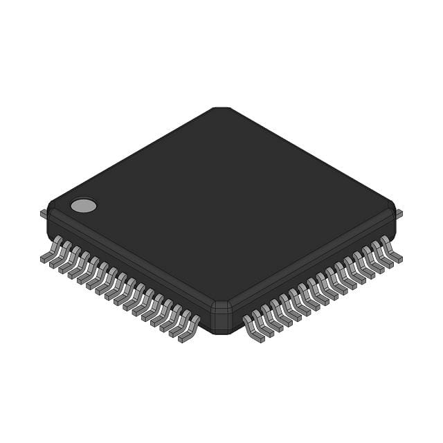
- Part No.:
- DS26504L
- Manufacturer:
- Analog Devices Inc./Maxim Integrated
- Category:
- Telecom
- Package:
- 64-LQFP
- Datasheet:
-
 DS26504L.pdf
- Description:
- T1/E1/J1/64KCC BITS ELEMENT
- Quantity:
- Payment:

- Shipping:

Inventory:458
Please send an inquiry. Send us your inquiry, and we will respond immediately.
Product details
Overview
DS26504L from Maxim Integrated is a building-integrated timing-supply (BITS) clock-recovery element and T1/E1/J1/64KCC transceiver. It recovers clocks from T1 (1.544MHz), E1 (2.048MHz), 64kHz composite clock (64KCC), and 6312kHz interfaces; supports SSM recovery/transmission in T1/E1 modes; operates from 3.3V supply with 5V-tolerant I/O; and is used in telecom central office timing distribution systems.
For engineers reviewing the DS26504L datasheet, DS26504L pinout, DS26504L application, or DS26504L equivalent, key selection criteria include G.703 compliance across multiple sync interfaces (64KCC, 6312kHz, E1, T1), independent transmit/receive rate conversion capability, hardware/software control flexibility (parallel/SPI/JTAG), and crystal-less jitter attenuation for T1/E1 line interfaces.
Technical Context
The DS26504L implements dual-path architecture with fully independent transmit and receive PLLs, enabling simultaneous rate translation between any supported input (e.g., 64KCC) and output (e.g., E1) synchronization rates. It integrates a G.703-compliant line interface unit (LIU) with software-selectable termination (75Ω/100Ω/110Ω/120Ω/133Ω) and supports both short- and long-haul operation via configurable line build-out.
Control is implemented through three parallel modes: 8-bit multiplexed/nonmultiplexed Intel/Motorola bus, SPI serial port (CPOL/CPHA configurable), and hardware mode using dedicated pins. JTAG boundary scan (IEEE 1149.1) provides test access, while status indications (LOS, AIS, LOF) are delivered on dedicated output pins.
Key Specifications
| Parameter | Value and Actual Design Meaning |
|---|---|
| Supply Voltage | 3.3V nominal; enables direct interfacing with modern 3.3V logic while maintaining 5V tolerance on all I/O pins for legacy system compatibility. |
| Synchronization Inputs | T1 (1.544MHz), E1 (2.048MHz), 64KCC (64kHz), 6312kHz, 8kHz, and 19.44MHz - supports multi-standard telecom timing hierarchy alignment. |
| SSM Handling | Receives and transmits T1 BOC SSM and E1 Sa(n) bit SSM with change-of-state detection and validation indication - meets GR-1244-CORE and ITU-T G.781 requirements. |
| Jitter Attenuation | Crystal-less jitter attenuator with bypass mode for T1/E1 operation - eliminates external crystal oscillator while meeting G.823/G.824 mask compliance. |
| Interface Standards | G.703 2048kHz, 64kHz Option A/B, Japanese Composite Clock, and 6312kHz interfaces - certified for global telecom infrastructure deployment. |
| Control Interfaces | 8-bit parallel (Intel/Motorola, multiplexed/nonmultiplexed), SPI serial, and hardware mode - allows flexible integration into diverse controller architectures without protocol translation. |
| Package | 64-pin LQFP (10mm × 10mm) - standard surface-mount footprint compatible with automated assembly and thermal management per θJA = 42°C/W (still air). |
Pinout & Package
DS26504L is housed in a 64-pin LQFP package (10mm × 10mm, 0.5mm pitch) with exposed thermal pad. Pin functions are defined per Maxim's DS26504 datasheet Rev 072308, Table 5-1 (LQFP Pinout).
| Pin/Terminal | Circuit Role | Design Meaning |
|---|---|---|
| CLKIN | Master Clock Input | Accepts 1.544MHz, 2.048MHz, 4.096MHz, 8.192MHz, 12.8MHz, or 16.384MHz MCLK - selects operating mode and frame timing reference. |
| TXCLK | Transmit Payload Clock Output | Provides recovered or synthesized payload clock synchronized to transmit data stream - essential for framer alignment in T1/E1 systems. |
| RXCLK | Receive Clock Output | Delivers recovered clock from incoming T1/E1/64KCC signal - used by downstream logic for data sampling and timing recovery. |
| LOS | Loss of Signal Indicator | Active-low open-drain output asserting when input signal amplitude falls below G.703-compliant threshold - enables immediate fault response in network elements. |
| AIS | Alarm Indication Signal Output | Active-high output signaling upstream alarm condition (e.g., remote failure) - conforms to T1/E1 framing standards for network management. |
| LOF | Loss of Frame Indicator | Active-low output indicating loss of valid frame alignment - critical for detecting framing errors in synchronous digital hierarchy applications. |
| TDO/TDI/TMS/TCK | JTAG Boundary Scan Interface | IEEE 1149.1 compliant test access port - enables production testing, in-system debugging, and configuration verification without intrusive probing. |
Key Features
| Feature | Design Value |
|---|---|
| GR-378 Composite Clock Compliance | Meets Telcordia GR-378-CORE requirements for BITS timing accuracy, stability, and holdover performance in central office environments. |
| Software-Selectable Termination | Internal 75Ω/100Ω/110Ω/120Ω/133Ω line termination selectable via register write - eliminates external resistor networks and simplifies board design across multiple cable types. |
| Monitor Mode for Bridging | Enables passive line monitoring without disrupting live traffic - supports network visibility and diagnostics in SONET/SDH add-drop multiplexers and cross-connect systems. |
| Fast Transmitter Disable | Dedicated hardware pin disables transmitter output within <1µs - protects downstream equipment during protection switching or fault isolation events. |
| Pin/Software Compatibility | Pin- and software-compatible with DS26502 and DS26503 - allows drop-in upgrade path within same product family for enhanced feature sets or temperature grade changes. |
Applications
| Central Office BITS Distribution | T1/E1 Line Card Timing |
|---|---|
Use Scenario: Distributing traceable, stratum-3-compliant timing from a primary reference source to multiple T1/E1 line cards in a carrier-class switch. IC Role / Device Role / Timing Role: BITS clock-recovery element translating 64KCC or 6312kHz input to synchronized T1/E1 outputs while recovering and regenerating SSM. Use Value: Ensures end-to-end synchronization integrity across heterogeneous TDM networks, meeting GR-1244-CORE and ITU-T G.781 SSM propagation requirements. | Use Scenario: Providing precise, jitter-attenuated clocking and SSM handling on modular T1/E1 interface cards in multiservice access platforms. IC Role / Device Role / Timing Role: Dual-function transceiver performing clock recovery, rate conversion, and SSM insertion/extraction for line-side physical layer interfacing. Use Value: Eliminates need for discrete jitter cleaners and separate SSM processors, reducing BOM count and PCB area while improving timing margin. |
| 64kHz Composite Clock Translation | Network Element Protection Switching |
Use Scenario: Converting legacy 64KCC timing signals to modern E1 or T1 sync interfaces in hybrid PSTN/NGN migration scenarios. IC Role / Device Role / Timing Role: Rate-conversion element accepting 64kHz composite clock and generating compliant E1 (2.048MHz) or T1 (1.544MHz) outputs with embedded SSM. Use Value: Enables seamless interworking between older BITS infrastructure and new packet-based transport layers without external frequency synthesizers. | Use Scenario: Supporting fast failover (<10ms) between primary and backup timing sources in mission-critical telecom nodes. IC Role / Device Role / Timing Role: Dual-input timing selector with hardware-controlled transmitter disable and LOS/LOF monitoring for autonomous switchover decisions. Use Value: Achieves sub-50ms hitless protection switching per ITU-T G.841, minimizing service interruption during clock source failures. |
Equivalent & Alternatives
The following parts are listed as comparable options for similar T1/E1/J1/64KCC timing and transceiver applications.
| Alternative Part | Technical Difference | Application Difference | Selection Advice |
|---|---|---|---|
| DS26503L | Lacks 6312kHz input support and Japanese 64kHz composite clock compliance; identical pinout and software interface. | Not suitable for Japanese telecom deployments requiring 6312kHz or J-64KCC; otherwise interchangeable in standard T1/E1/64KCC systems. | Select DS26503L only when 6312kHz and J-64KCC features are unnecessary - reduces cost while retaining full T1/E1/64KCC functionality. |
| DS26502L | Does not support SSM transmission in E1 mode; no 6312kHz input; limited termination options (75Ω/120Ω only). | Cannot meet full G.781 SSM propagation requirements in E1 networks; unsuitable for applications requiring bidirectional SSM or Japanese sync standards. | Choose DS26502L for basic T1/E1 clock recovery where SSM regeneration and extended sync interface support are not required. |
Compared with DS26503L and DS26502L, the DS26504L delivers full global telecom sync interface coverage (including 6312kHz and J-64KCC), complete SSM handling for both T1 and E1, and expanded termination flexibility - making it the only variant qualified for stratum-3 BITS applications across North America, Europe, and Japan.
Availability
DS26504L is available at Aetrix Electronics and suitable for central office timing distribution, T1/E1 line card design, and telecom infrastructure upgrades requiring stable component supply, long-term lifecycle assurance, and full G.703/G.781 compliance.
Supply support for DS26504L includes scheduled delivery planning, volume procurement assistance, BOM continuity management, traceable sourcing, and lifecycle availability coordination for OEM customers, industrial embedded developers, connected-device designers, and electronics production programs.
Manufacturer
Maxim Integrated (now part of Analog Devices) is a semiconductor company specializing in precision analog, mixed-signal, and high-reliability ICs for communications, industrial, and automotive markets.
The DS26504L belongs to Maxim's telecom timing and interface product line, designed specifically for building-integrated timing supply (BITS) systems and T1/E1/J1 physical layer synchronization in carrier-grade network equipment.
FAQ
What is the operating temperature range for the DS26504L?
The DS26504L is specified for operation from 0°C to +70°C. This commercial temperature grade makes it suitable for controlled-environment telecom infrastructure such as central office line cards and indoor network elements. The DS26504LN variant extends this to –40°C to +85°C for extended-temperature applications. DS26504L maintains full G.703 compliance and jitter performance across its rated range.
Does the DS26504L support both T1 and E1 Synchronization Status Message (SSM) handling?
Yes, the DS26504L fully supports SSM in both T1 and E1 modes: it receives and validates T1 BOC SSM and E1 Sa(n) bit SSM, and transmits regenerated SSM with change-of-state indication. This meets ITU-T G.781 requirements for SSM propagation in hierarchical timing networks. DS26504L is the only device in the DS2650x family to provide bidirectional SSM for E1.
Can the DS26504L operate without an external crystal oscillator?
Yes, the DS26504L includes a crystal-less jitter attenuator for T1 and E1 operation, eliminating the need for an external crystal. It uses internal PLLs locked to the incoming line signal or master clock to achieve G.823/G.824-compliant jitter performance. The device also supports bypass mode for direct clock pass-through when ultra-low latency is required.
What control interfaces does the DS26504L support?
The DS26504L supports three independent control interfaces: an 8-bit parallel port (configurable for Intel or Motorola timing, multiplexed or nonmultiplexed), a 4-wire SPI serial port (with configurable CPOL/CPHA), and a hardware control mode using dedicated pins. All interfaces provide full register-level access to configuration, status, and diagnostic functions without requiring external protocol translation logic.
Is the DS26504L pin-compatible with other devices in the DS2650x family?
Yes, the DS26504L is pin- and software-compatible with the DS26502L and DS26503L. This allows direct replacement in existing designs to upgrade functionality - for example, adding 6312kHz support or full E1 SSM transmission - without PCB layout changes. Firmware and driver code remain fully reusable across the family.
DS26504L Specifications
- Product attributes
- Attribute value
- Manufacturer:
- Analog Devices Inc./Maxim Integrated
- Series:
- -
- Package/Case:
- 64-LQFP
- Packaging:
- Bulk
- Product Status:
- Obsolete
- Function:
- BITS Element
- Interface:
- 64KCC, E1, J1, T1
- Number of Circuits:
- 1
- Voltage - Supply:
- 3.135V ~ 3.465V
- Current - Supply:
- 150mA
- Power (Watts):
- -
- Operating Temperature:
- 0°C ~ 70°C
- Grade:
- -
- Qualification:
- -
- Mounting Type:
- Surface Mount
- Supplier Device Package:
- 64-LQFP (10x10)
DS26504L FAQ
1.How can I place an order for DS26504L through Aetrix?
Please submit a Request for Quotation (RFQ) for DS26504L on Aetrix. Our sales agent will provide a competitive quotation and guide you through the order confirmation once you accept the terms.
2.Are the price and stock information for DS26504L reliable?
The price and inventory of DS26504L are updated periodically and may fluctuate due to market conditions. Stock and pricing data are typically refreshed every 24 hours. Quotation validity for DS26504L is usually 5 days.
3.What payment methods are accepted for DS26504L?
We accept Wire Transfer, PayPal, Credit Card, Western Union, MoneyGram, and Escrow for DS26504L transactions.
Note: Certain payment methods may incur a processing fee.
4.How is shipping managed for DS26504L?
DS26504L orders can be shipped via leading logistics carriers, including DHL, UPS, FedEx, TNT, or Registered Mail.
Once your DS26504L order is processed, you will receive an email with the shipment details and tracking number.
Note: Tracking information may take up to 24 hours to appear. Express delivery typically takes 3–5 business days.
5.How can I obtain technical support or documentation for DS26504L?
For technical support, including DS26504L datasheets, pinout diagrams, or application guidance, please contact our engineering support team. They can provide detailed documentation and assistance for your DS26504L requirements.
6.How does Aetrix verify that DS26504L is sourced from the original manufacturer or authorized distributors?
All DS26504L products on Aetrix are procured from qualified distributors and authorized channels. Our dedicated quality assurance team conducts strict verification, including traceability checks and, if necessary, third-party testing. This ensures that DS26504L meets industry standards.
7.What is the process for return or replacement of DS26504L?
All DS26504L units undergo pre-shipment inspection (PSI). If there is an issue with DS26504L, returns or replacements are accepted under the following conditions:
1.Quantity discrepancies, incorrect items, or visible external defects (such as breakage or corrosion), acknowledged by Aetrix.
2.The issue is reported within 90 days of delivery.
3.The DS26504L part is unused and in its original packaging.
Return procedure for DS26504L:
1.Submit a request within 90 days.
2.Obtain a Return Material Authorization (RMA) from Aetrix.
DS26504L Tags

-
LMC567CMX/NOPB
Texas Instruments
-
LM567CMX/NOPB
Texas Instruments
-
LM567CM/NOPB
Texas Instruments

-
VSC8531XMW-02
Microchip Technology
-
VSC8531XMW-05
Microchip Technology

-
GPY115C0VI
MaxLinear, Inc.

-
SI32185-A-FMR
Skyworks Solutions Inc.

-
VSC8541XMV-05
Microchip Technology

-
SI32178-B-FM1R
Skyworks Solutions Inc.
-
GPY215C0VI
MaxLinear, Inc.

-
CPC7514ZTR
Littelfuse Inc.

-
VSC8502XML-03
Microchip Technology
Tech Hub

A practical engineering guide to 3.3V and 5V logic compatibility, input thresholds, resistor dividers, translator ICs, MOSFET level shifting, I2C pull-ups, timing limits and power-sequencing risks.

The 74HC595 uses push-pull logic outputs, while the TPIC6B595 uses 50 V open-drain DMOS sinks for higher-power loads. This guide compares timing, current limits, 3.3 V interfacing, load wiring, thermal…

The 74HC595 converts serial data into eight stable parallel outputs. This guide covers pin functions, shift and storage timing, OE and MR behavior, drive-current limits, cascading, voltage compatibilit…

A technical comparison of level-sensitive latches and edge-triggered flip-flops, covering timing windows, setup and hold limits, master–slave operation, time borrowing, race-through, HDL inference and…

A D latch stores one bit while Enable controls when data can pass. This reference covers gate-level operation, truth tables, transparency, setup and hold timing, LE versus OE, common ICs and practical …

An SR latch stores one bit through cross-coupled feedback. This engineering reference covers NOR and NAND implementations, truth tables, forbidden-state recovery, gated operation, switch debouncing, fa…

Latch circuits retain one bit through feedback. This technical reference covers SR and D latches, truth tables, transparency, timing limits, latch-versus-flip-flop behavior, applications and common log…

An engineering guide to LED driver operation, constant-current and constant-voltage outputs, linear and switching topologies, dimming, IC selection, calculations, replacement compatibility, and fault c…

Operational amplifier guide covering op amp basics, feedback, ideal vs real op amps, common configurations, buffer circuits, offset, bias current, gain-bandwidth, slew rate, rail-to-rail limits and sel…

Jumper cables guide covering safe connection order, red and black clamp placement, final ground connection, cable gauge, length, clamp quality, copper vs CCA cables, jump starter comparison and battery…


