
 My Inquiry
 My Account


Analog Devices Inc./Maxim Integrated DS2760E8000001/T&R
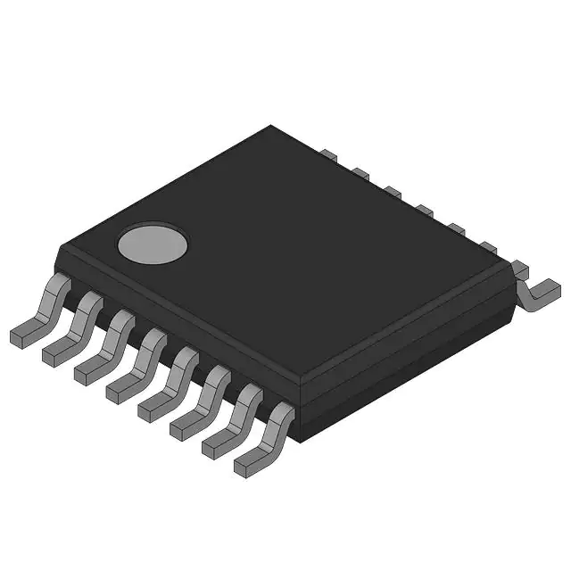
- Part No.:
- DS2760E8000001/T&R
- Manufacturer:
- Analog Devices Inc./Maxim Integrated
- Category:
- Battery Management
- Package:
- 16-TSSOP (0.173", 4.40mm Width)
- Datasheet:
-
 DS2760E8000001/T&R.pdf
- Description:
- IC BATT MONITOR PRECISION LI+
- Quantity:
- Payment:

- Shipping:

Inventory:6,000
Please send an inquiry. Send us your inquiry, and we will respond immediately.
Product details
Overview
DS2760E8000001/T&R from Maxim Integrated is a high-precision Li+ battery monitor IC with integrated 25mΩ internal sense resistor, 12-bit bidirectional current measurement (±1.9A, 0.625mA LSB), 4.88mV voltage resolution, and 0.125°C temperature resolution via on-chip sensor. It delivers overvoltage, undervoltage, and overcurrent/short-circuit protection for single-cell lithium-ion packs in portable medical devices and power tools.
For engineers reviewing the DS2760E8000001/T&R datasheet, DS2760E8000001/T&R pinout, DS2760E8000001/T&R application, or DS2760E8000001/T&R equivalent, key selection criteria include its 1-Wire interface with unique 64-bit address, zero-volt battery recovery charge path, lockable EEPROM for secure battery data storage, and programmable I/O for pack-level control of LEDs or switches.
Technical Context
The DS2760E8000001/T&R implements a dedicated analog front-end with dual current-sense inputs (IS1/IS2), voltage sensing on VIN, and thermal sensing via integrated silicon diode. Its protection logic uses configurable thresholds-including 4.275V overvoltage and undervoltage detection-with fixed delays (tOVD, tUVD) and automatic FET gate control via CC/DC outputs.
It operates in two power modes: Active Mode (90μA max) for continuous measurement and accumulation, and Sleep Mode (2μA max) triggered by DQ low >2s, VIN < VUV, or SWAP command. Recovery from deep discharge is enabled via PLS-to-VDD current-limited path when VDD < 3V.
Key Specifications
| Parameter | Value and Actual Design Meaning |
|---|---|
| Current Measurement | 12-bit bidirectional, ±1.9A range, 0.625mA LSB with internal 25mΩ sense resistor |
| Voltage Resolution | 4.88mV LSB over 0–4.75V range, stored in two's-complement Voltage Register (addresses 0C–0D) |
| Temperature Resolution | 0.125°C LSB over –40°C to +127°C, using integrated on-die sensor (addresses 18–19) |
| Protection Thresholds | Overvoltage = 4.275V, Undervoltage = 2.5V, Overcurrent = ±1.9A (configurable via EEPROM) |
| Memory Resources | 32 bytes lockable EEPROM (blocks 0/1), 16 bytes SRAM, all accessible via 1-Wire interface |
| Power Consumption | 90μA max active current; 2μA max sleep current; supports battery-powered long-life operation |
| Interface | Dallas 1-Wire® (single-conductor, open-drain DQ), factory-programmed 64-bit unique address (family code 30h) |
Pinout & Package
DS2760E8000001/T&R is housed in a 16-pin TSSOP package (JEDEC MO-153, 5mm × 4.4mm × 1.2mm). Pin assignments are validated per Maxim's official mechanical drawing 16tssop.pdf and DS2760 datasheet Rev. 0, with pins 11/12/13 as VSS ground connections and SNS connected to internal 25mΩ sense resistor.
| Pin/Terminal | Circuit Role | Design Meaning |
|---|---|---|
| CC | Charge Control Output | Drives external p-channel high-side FET gate to disable charging during overvoltage or charge overcurrent |
| DC | Discharge Control Output | Drives external p-channel high-side FET gate to disable discharging during undervoltage, discharge overcurrent, or short circuit |
| DQ | 1-Wire Data I/O | Single-wire bidirectional communication line with internal 1μA pull-down; enables multi-device daisy-chain on shared bus |
| PIO | Programmable I/O | Open-drain output/input controllable via Special Feature Register; used for LED drive or switch monitoring in battery pack |
| PLS | Pack Positive Terminal Input | Monitors charger attachment; provides recovery charge path from PLS to VDD when cell is deeply depleted (VDD < 3V) |
| PS | Power Switch Sense Input | Internally pulled to VDD with 1μA source; detects low-impedance connection to VSS to wake device from Sleep Mode |
| VIN | Voltage Sense Input | Measures cell voltage referenced to VSS; weak internal pull-up to VDD ensures valid reading during low-power states |
| VDD | Power Supply Input | Accepts 2.5V–5.5V supply from Li+ cell anode; powers internal circuitry and bias networks |
| VSS | Device Ground | Primary reference for all analog measurements; connects directly to Li+ cell cathode; pins 11/12/13 are bonded internally |
| SNS | Sense Resistor Connection | Connects to negative terminal of battery pack; internal 25mΩ resistor bridges SNS–VSS in this variant |
| IS1 / IS2 | Current Sense Inputs | Filter inputs (4.7kΩ + 0.1μF) measuring differential voltage across sense element; define VIS = VIS1 – VIS2 for bidirectional current sign |
Key Features
| Feature | Design Value |
|---|---|
| Zero-Volt Battery Recovery | Enables safe reactivation of deeply discharged cells (<0.5V) via controlled PLS→VDD current path without external circuitry |
| Lockable EEPROM Security | Two 16-byte blocks (20h–2Fh, 30h–3Fh) can be permanently locked to ROM to protect calibration data and protection defaults |
| 1-Wire Multi-Drop Support | Unique 64-bit address allows up to 10+ DS2760E8000001/T&R units on single DQ line-ideal for multi-cell smart battery packs |
| Integrated Temperature Sensing | Eliminates need for external thermistor or NTC; on-die sensor calibrated to ±2°C accuracy over full operating range |
| Current Accumulation Engine | Hardware-based accumulator (addresses 10h–11h) tracks net charge flow in 0.25mAh increments for precise remaining capacity estimation |
Applications
| Portable Medical Devices | Power Tools |
|---|---|
Use Scenario: Rechargeable Li+ battery pack in handheld ultrasound or infusion pump requiring safety-critical overvoltage and short-circuit protection. IC Role / Device Role / Timing Role: Primary safety monitor and data acquisition node; performs real-time current accumulation and voltage trending for runtime prediction. Use Value: Enables FDA-compliant battery management with traceable EEPROM-stored calibration and fault logs, reducing BOM count by eliminating discrete sense resistors and thermistors. | Use Scenario: High-current 18V Li+ pack in cordless drill where rapid discharge protection and temperature monitoring prevent thermal runaway. IC Role / Device Role / Timing Role: Central protection controller interfacing with host MCU via 1-Wire; triggers DC FET shutdown within tSCD < 10ms during short circuit. Use Value: Delivers sub-10ms short-circuit response and 0.125°C temperature granularity-critical for detecting localized cell heating before catastrophic failure. |
| Wearable Fitness Trackers | Enterprise Two-Way Radios |
Use Scenario: Ultra-low-power wearable with coin-cell-sized Li+ battery needing extended shelf life and accurate state-of-charge reporting. IC Role / Device Role / Timing Role: Low-quiescent monitor in Sleep Mode (2μA); wakes on PS pin event or DQ activity to report accumulated current and voltage. Use Value: Extends shelf life beyond 12 months while maintaining ±2% SOC accuracy via hardware current integration and temperature-compensated offset correction. | Use Scenario: Ruggedized radio battery pack operating in extreme temperatures (-20°C to +60°C) requiring reliable undervoltage lockout and recovery. IC Role / Device Role / Timing Role: Safety supervisor enforcing VUV = 2.5V cutoff and enabling zero-volt recovery only when PLS voltage exceeds VDD – VTP. Use Value: Prevents irreversible copper shunting in cold environments by enforcing strict undervoltage release conditions and providing controlled recharge current (IRC). |
Equivalent & Alternatives
The following parts are listed as comparable options for similar Li+ battery monitoring applications.
| Alternative Part | Technical Difference | Application Difference | Selection Advice |
|---|---|---|---|
| BQ27426YZFT | TI fuel gauge with impedance tracking; no integrated protection FET drivers; requires external protection IC | Lacks CC/DC outputs-must pair with separate protector like BQ29700; adds PCB area and complexity | Select when advanced SOC modeling (impedance spectroscopy) is prioritized over integrated safety control |
| MAX17048G+T | Maxim standalone fuel gauge; 14-bit current ADC; no internal sense resistor; higher active current (120μA) | No overvoltage/undervoltage protection logic or FET drive capability-pure metrology device | Select when precise coulomb counting is required but protection is handled by companion IC or system-level firmware |
Compared with BQ27426YZFT and MAX17048G+T, DS2760E8000001/T&R uniquely integrates precision metrology, configurable protection logic, and FET drive outputs in one TSSOP package-reducing bill-of-materials and simplifying compliance-critical safety architecture.
Availability
DS2760E8000001/T&R is available at Aetrix Electronics and suitable for portable medical devices, power tools, wearables, and enterprise radios requiring stable component supply, long-term lifecycle support, and traceable sourcing for ISO 13485 and IEC 62366 programs.
Supply support for DS2760E8000001/T&R includes scheduled delivery planning, volume procurement assistance, BOM continuity management, traceable sourcing, and lifecycle availability coordination for OEM customers, industrial embedded developers, connected-device designers, and electronics production programs.
Manufacturer
Maxim Integrated (now part of Analog Devices) designs precision analog, mixed-signal, and power management ICs for demanding industrial, medical, and automotive applications.
The DS2760 product line targets cost-sensitive, space-constrained Li+ battery packs requiring integrated safety monitoring, metrology, and 1-Wire communication-enabling smart battery functionality without external microcontrollers.
FAQ
What is the overvoltage protection threshold for DS2760E8000001/T&R?
The DS2760E8000001/T&R has a factory-configured overvoltage threshold of 4.275V, with a typical overvoltage delay (tOVD) of 1 second. This value is stored in EEPROM and can be modified by the host system via the Protection Register. The DS2760E8000001/T&R asserts the CC output high to disable charging when VIN exceeds this threshold for longer than tOVD, preventing Li+ cell damage during fast charging.
Does DS2760E8000001/T&R support zero-volt battery recovery?
Yes, DS2760E8000001/T&R supports zero-volt battery recovery through its PLS-to-VDD current-limited path. When VDD drops below 3V (e.g., due to deep discharge), the DS2760E8000001/T&R enables a controlled recovery charge current (IRC) from PLS to VDD. This safely raises VDD to operational levels before allowing normal charge FET activation-eliminating need for external recovery circuitry.
How does DS2760E8000001/T&R handle current measurement accuracy across temperature?
DS2760E8000001/T&R performs continuous internal compensation for current measurement offset caused by temperature and voltage variations. It also supports user-programmable offset bias (stored at EEPROM address 33h) in two's-complement format, applied to both internal and external sense resistor configurations. This ensures <±1% current measurement error over –40°C to +85°C ambient without external calibration.
Can DS2760E8000001/T&R operate with multiple units on a single 1-Wire bus?
Yes, DS2760E8000001/T&R supports multi-drop 1-Wire operation. Each unit has a unique factory-programmed 64-bit address (family code 30h), allowing up to 10+ devices on one DQ line. The host system selects individual DS2760E8000001/T&R units using the Match ROM command, enabling centralized monitoring of multi-cell battery packs without additional addressing hardware.
What memory types are available on DS2760E8000001/T&R and how are they used?
DS2760E8000001/T&R provides three memory types: 32 bytes of lockable EEPROM (blocks 0/1), 16 bytes of general-purpose SRAM, and register-mapped instrumentation memory. EEPROM stores critical nonvolatile data (e.g., protection defaults, calibration offsets); lockable blocks prevent accidental overwrite. SRAM holds temporary runtime data. All memory is accessed via 1-Wire commands-Read Data, Write Data, Copy Data, and Recall Data-with shadow RAM ensuring glitch-free writes.
DS2760E8000001/T&R Specifications
- Product attributes
- Attribute value
- Manufacturer:
- Analog Devices Inc./Maxim Integrated
- Series:
- -
- Package/Case:
- 16-TSSOP (0.173", 4.40mm Width)
- Packaging:
- Bulk
- Product Status:
- Obsolete
- Function:
- Battery Monitor
- Battery Chemistry:
- Lithium Ion
- Number of Cells:
- 1
- Fault Protection:
- Over Current, Over/Under Voltage, Short Circuit
- Interface:
- 1-Wire
- Operating Temperature:
- -40°C ~ 85°C
- Grade:
- -
- Qualification:
- -
- Mounting Type:
- Surface Mount
- Supplier Device Package:
- 16-TSSOP
DS2760E8000001/T&R FAQ
1.How can I place an order for DS2760E8000001/T&R through Aetrix?
Please submit a Request for Quotation (RFQ) for DS2760E8000001/T&R on Aetrix. Our sales agent will provide a competitive quotation and guide you through the order confirmation once you accept the terms.
2.Are the price and stock information for DS2760E8000001/T&R reliable?
The price and inventory of DS2760E8000001/T&R are updated periodically and may fluctuate due to market conditions. Stock and pricing data are typically refreshed every 24 hours. Quotation validity for DS2760E8000001/T&R is usually 5 days.
3.What payment methods are accepted for DS2760E8000001/T&R?
We accept Wire Transfer, PayPal, Credit Card, Western Union, MoneyGram, and Escrow for DS2760E8000001/T&R transactions.
Note: Certain payment methods may incur a processing fee.
4.How is shipping managed for DS2760E8000001/T&R?
DS2760E8000001/T&R orders can be shipped via leading logistics carriers, including DHL, UPS, FedEx, TNT, or Registered Mail.
Once your DS2760E8000001/T&R order is processed, you will receive an email with the shipment details and tracking number.
Note: Tracking information may take up to 24 hours to appear. Express delivery typically takes 3–5 business days.
5.How can I obtain technical support or documentation for DS2760E8000001/T&R?
For technical support, including DS2760E8000001/T&R datasheets, pinout diagrams, or application guidance, please contact our engineering support team. They can provide detailed documentation and assistance for your DS2760E8000001/T&R requirements.
6.How does Aetrix verify that DS2760E8000001/T&R is sourced from the original manufacturer or authorized distributors?
All DS2760E8000001/T&R products on Aetrix are procured from qualified distributors and authorized channels. Our dedicated quality assurance team conducts strict verification, including traceability checks and, if necessary, third-party testing. This ensures that DS2760E8000001/T&R meets industry standards.
7.What is the process for return or replacement of DS2760E8000001/T&R?
All DS2760E8000001/T&R units undergo pre-shipment inspection (PSI). If there is an issue with DS2760E8000001/T&R, returns or replacements are accepted under the following conditions:
1.Quantity discrepancies, incorrect items, or visible external defects (such as breakage or corrosion), acknowledged by Aetrix.
2.The issue is reported within 90 days of delivery.
3.The DS2760E8000001/T&R part is unused and in its original packaging.
Return procedure for DS2760E8000001/T&R:
1.Submit a request within 90 days.
2.Obtain a Return Material Authorization (RMA) from Aetrix.
DS2760E8000001/T&R Tags

-
BQ29700DSER
Texas Instruments

-
S-8241ABKMC-GBKT2G
ABLIC Inc.
-
S-8241ABPMC-GBPT2G
ABLIC Inc.

-
BQ27427YZFR
Texas Instruments

-
BQ27426YZFR
Texas Instruments

-
STC3117IJT
STMicroelectronics

-
STC3115IJT
STMicroelectronics

-
BQ76925RGER
Texas Instruments
-
NPM1100-QDAA-R
Nordic Semiconductor ASA

-
BQ27441DRZR-G1A
Texas Instruments

-
STC3115AIQT
STMicroelectronics

-
S-8252AAL-M6T1U
ABLIC Inc.
Tech Hub

A practical engineering guide to 3.3V and 5V logic compatibility, input thresholds, resistor dividers, translator ICs, MOSFET level shifting, I2C pull-ups, timing limits and power-sequencing risks.

The 74HC595 uses push-pull logic outputs, while the TPIC6B595 uses 50 V open-drain DMOS sinks for higher-power loads. This guide compares timing, current limits, 3.3 V interfacing, load wiring, thermal…

The 74HC595 converts serial data into eight stable parallel outputs. This guide covers pin functions, shift and storage timing, OE and MR behavior, drive-current limits, cascading, voltage compatibilit…

A technical comparison of level-sensitive latches and edge-triggered flip-flops, covering timing windows, setup and hold limits, master–slave operation, time borrowing, race-through, HDL inference and…

A D latch stores one bit while Enable controls when data can pass. This reference covers gate-level operation, truth tables, transparency, setup and hold timing, LE versus OE, common ICs and practical …

An SR latch stores one bit through cross-coupled feedback. This engineering reference covers NOR and NAND implementations, truth tables, forbidden-state recovery, gated operation, switch debouncing, fa…

Latch circuits retain one bit through feedback. This technical reference covers SR and D latches, truth tables, transparency, timing limits, latch-versus-flip-flop behavior, applications and common log…

An engineering guide to LED driver operation, constant-current and constant-voltage outputs, linear and switching topologies, dimming, IC selection, calculations, replacement compatibility, and fault c…

Operational amplifier guide covering op amp basics, feedback, ideal vs real op amps, common configurations, buffer circuits, offset, bias current, gain-bandwidth, slew rate, rail-to-rail limits and sel…

Jumper cables guide covering safe connection order, red and black clamp placement, final ground connection, cable gauge, length, clamp quality, copper vs CCA cables, jump starter comparison and battery…


