
 My Inquiry
 My Account


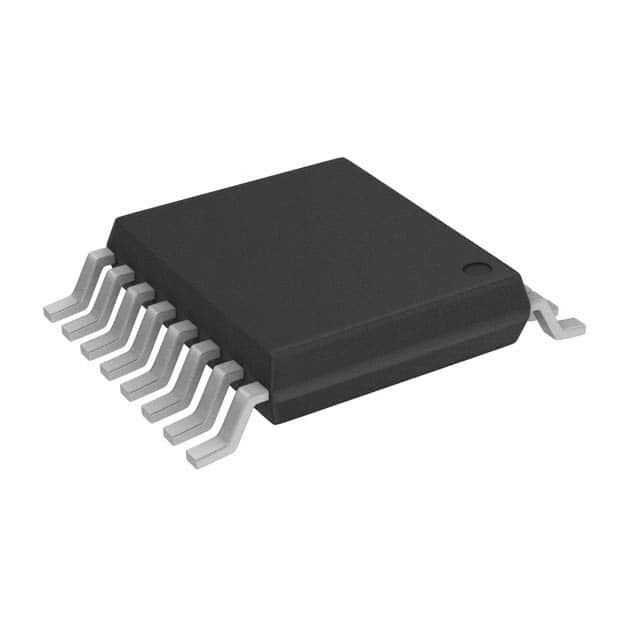
Analog Devices Inc./Maxim Integrated DS2764BE+T&R
- Part No.:
- DS2764BE+T&R
- Manufacturer:
- Analog Devices Inc./Maxim Integrated
- Category:
- Battery Management
- Package:
- 16-TSSOP (0.173", 4.40mm Width)
- Datasheet:
-
 DS2764BE+T&R.pdf
- Description:
- IC BATT MONITOR LI-ION 16TSSOP
- Quantity:
- Payment:

- Shipping:

Inventory:2,777
Please send an inquiry. Send us your inquiry, and we will respond immediately.
Product details
Overview
DS2764BE+T&R from Maxim Integrated is a high-precision Li+ battery monitor IC with integrated 25mΩ sense resistor, 12-bit bidirectional current measurement (±1.9A, 0.625mA LSB), 4.88mV voltage resolution, and 0.125°C temperature resolution. It performs real-time safety protection (overvoltage, undervoltage, overcurrent, short-circuit), current accumulation (0.25mAh LSB), and stores battery data in 40 bytes of lockable EEPROM - deployed in smartphone and PDA battery packs for remaining capacity estimation and cell-level safety monitoring.
For engineers reviewing the DS2764BE+T&R datasheet, DS2764BE+T&R pinout, DS2764BE+T&R application, or DS2764BE+T&R equivalent, this page delivers verified technical context, exact pin functions, protection timing thresholds (e.g., tOVD = 1s, tSCD = 200µs), internal vs. external sense resistor configuration trade-offs, and validated alternative parts for battery pack design continuity.
Technical Context
The DS2764BE+T&R implements a dedicated analog front-end with on-die temperature sensor, precision voltage reference, and programmable gain amplifier for current sensing across IS1/IS2. Its protection logic executes autonomous state transitions - e.g., CC high on VIN > 4.35V for ≥1s triggers charge FET disable, while DC high on VSNS > 200mV for ≥200µs disables discharge FET.
It operates in two power modes: active mode (60µA typical) for continuous measurement and protection, and sleep mode (1µA typical) entered after 2.1s bus inactivity or VIN < 2.6V. Wake-up sources include PS pin pull-down, PLS-to-VDD charger detection, or SCL/SDA activity - enabling zero-power standby in disconnected battery packs.
Key Specifications
| Parameter | Value and Actual Design Meaning |
|---|---|
| Supply Voltage | 2.5V to 5.5V - supports direct connection to single-cell Li+ (2.7–4.2V) with margin for transient spikes. |
| Current Measurement | ±1.9A dynamic range, 0.625mA LSB - enables accurate coulomb counting for sub-1% capacity error in smartphones. |
| Voltage Resolution | 4.88mV - resolves 0.1% of 4.8V full-scale, sufficient for precise SOC estimation via OCV lookup. |
| Temperature Resolution | 0.125°C - detects thermal runaway onset early enough to trigger protective shutdown before cell damage. |
| Overvoltage Delay | 1s typical - prevents nuisance tripping during brief charge voltage overshoots while ensuring fast response to sustained faults. |
| Sleep Current | 1µA typical - extends shelf life of sealed battery packs by minimizing self-discharge over months of storage. |
| EEPROM Size | 40 bytes, lockable per block - stores calibrated parameters, cycle count, and manufacturer data with permanent write-protection. |
Pinout & Package
DS2764BE+T&R is packaged in a 16-pin TSSOP (lead-free/RoHS-compliant) with 0.65mm pitch and exposed thermal pad. Pin functions are validated per Maxim's official datasheet (Rev. 0, pp.6–7).
| Pin/Terminal | Circuit Role | Design Meaning |
|---|---|---|
| CC (Pin 1) | Charge Protection Control Output | Drives gate of external P-channel high-side charge FET; open-drain, VPLS-referenced output ensures safe turn-off during overvoltage. |
| PLS (Pin 2) | Battery Pack Positive Terminal Input | Monitors pack+ for overload removal and charger presence; provides recovery charge path from PLS to VDD when cell is deeply depleted. |
| DC (Pin 3) | Discharge Protection Control Output | Drives gate of external P-channel high-side discharge FET; asserts high during short-circuit (tSCD = 200µs) to limit fault energy. |
| SNS (Pins 4,5,6) | Sense Resistor Connection | Connects to battery negative terminal; internal 25mΩ resistor bridges VSS–SNS - eliminates BOM cost and layout area for discrete sense element. |
| PS (Pin 7) | Power Switch Sense Input | Wakes device from sleep on pull-down to VSS; enables mechanical power switch integration without host MCU intervention. |
| IS2 (Pin 8) | Current-Sense Input | Internally tied to SNS via 4.7kΩ; forms low-pass filter with IS1 capacitor to reject switching noise from DC-DC converters. |
| IS1 (Pin 9) | Current-Sense Input | Internally tied to VSS via 4.7kΩ; differential pair with IS2 measures voltage drop across sense resistor for bidirectional current detection. |
| SDA (Pin 10) | 2-Wire Serial Data I/O | Open-drain interface with 1µA pulldown - detects cable disconnection and supports multi-drop battery pack configurations. |
| VSS (Pins 11,12,13) | Device Ground | Must connect directly to Li+ cell negative; serves as current-sense reference and protection circuit return path. |
| SCL (Pin 14) | 2-Wire Serial Clock Input | Input-only clock line with 1µA pulldown; timing compliant with 100kHz I²C standard (tLOW ≥ 4.7µs, tHIGH ≥ 4.0µs). |
| VDD (Pin 15) | Power-Supply Input | Powered from Li+ cell positive; decoupling required near pin to suppress noise coupling into analog measurement paths. |
| VIN (Pin 16) | Voltage Sense Input | Monitors cell voltage with weak internal pull-up to VDD; input impedance >5MΩ minimizes loading on high-impedance divider networks. |
Key Features
| Feature | Design Value |
|---|---|
| Integrated 25mΩ sense resistor | Eliminates external component, reduces PCB area by ~3mm², and avoids tolerance/TC errors of discrete resistors. |
| 0V battery recovery charge path | Enables charging of fully depleted cells (<1.5V) via PLS-to-VDD current source, restoring communication before main charge begins. |
| Lockable EEPROM blocks | Two 16-byte and one 8-byte block - allows permanent write-protection of calibration data while retaining field-updatable usage logs. |
| Programmable 7-bit I²C slave address | Supports up to 128 devices on same bus - essential for multi-cell battery packs requiring individual cell monitoring. |
| Soft-start discharge FET control | Gradually ramps DC output on wake-up to limit inrush current when inserting battery into unpowered host system. |
Applications
| Smartphone Battery Management | PDA Power Monitoring |
|---|---|
|
Use Scenario: Real-time tracking of charge/discharge cycles, temperature rise during fast charging, and voltage sag under RF transmit load. IC Role / Device Role / Timing Role: Primary battery monitor providing coulomb counting, safety cutoff, and 2-wire telemetry to baseband processor. Use Value: Enables accurate remaining capacity reporting (<3% error) and prevents thermal runaway by triggering shutdown at 60°C. |
Use Scenario: Long-term logging of battery health metrics (cycle count, max discharge rate, capacity fade) across 2+ years of field use. IC Role / Device Role / Timing Role: Standalone data logger with nonvolatile EEPROM storage, operating autonomously during host sleep. Use Value: Preserves battery history even after deep discharge or accidental short, supporting predictive maintenance and warranty analytics. |
| Digital Camera Power Safety | Portable Medical Device Backup |
|
Use Scenario: Instantaneous current surge detection during flash capacitor charging and motor-driven lens actuation. IC Role / Device Role / Timing Role: Overcurrent protector with 20ms response (tOCD) and short-circuit detector with 200µs latency (tSCD). Use Value: Prevents MOSFET failure and fire hazard by disabling discharge path before energy dissipation exceeds SOA limits. |
Use Scenario: Maintaining safe operation of life-critical devices (e.g., portable insulin pumps) during unexpected low-voltage conditions. IC Role / Device Role / Timing Role: Undervoltage supervisor with 100ms delay (tUVD) and automatic recovery charge activation below 2.6V. Use Value: Ensures uninterrupted therapy delivery by restoring power to microcontroller before cell voltage collapses irreversibly. |
Equivalent & Alternatives
The following parts are listed as comparable options for similar Li+ battery monitor applications.
| Alternative Part | Technical Difference | Application Difference | Selection Advice |
|---|---|---|---|
| BQ27426YZFT | Higher accuracy (0.5% SOC error), integrated fuel gauge algorithm, but no internal sense resistor - requires external 10mΩ. | Targets premium smartphones needing factory-calibrated fuel gauging; lacks DS2764BE+T&R's 0V recovery and simple register-map interface. | Select BQ27426YZFT when algorithmic SOC accuracy outweighs BOM simplicity and deep-discharge recovery capability. |
| MAX17048G+T | 1% SOC accuracy, ModelGauge™ m3 algorithm, 1.8V–4.5V supply, but only 20µA active current - no integrated protection FET drivers. | Used in wearables where ultra-low power dominates; requires external protection ICs, increasing solution size and complexity. | Choose MAX17048G+T for space-constrained designs where standalone fuel gauging suffices and protection is handled separately. |
Compared with DS2764BE+T&R, BQ27426YZFT offers superior SOC modeling but adds external sense resistor dependency and removes autonomous 0V recovery, while MAX17048G+T reduces power consumption by 67% yet shifts protection responsibility to external components - making DS2764BE+T&R optimal for cost-sensitive, self-contained battery packs requiring integrated safety and deep-discharge resilience.
Availability
DS2764BE+T&R is available at Aetrix Electronics and suitable for smartphone battery packs, PDA power systems, and digital camera backup power requiring stable component supply, long-term lifecycle support, and RoHS-compliant packaging.
Supply support for DS2764BE+T&R includes scheduled delivery planning, volume procurement assistance, BOM continuity management, traceable sourcing, and lifecycle availability coordination for OEM customers, industrial embedded developers, connected-device designers, and electronics production programs.
Manufacturer
Maxim Integrated (now part of Analog Devices) designs precision analog and mixed-signal ICs for power management, sensing, and connectivity - with emphasis on reliability and integration for portable electronics.
The DS2764BE+T&R belongs to Maxim's battery fuel gauge and protection product line, engineered specifically for cost-sensitive single-cell Li+ battery packs needing autonomous safety, accurate capacity tracking, and minimal external components.
FAQ
What is the primary function of the DS2764BE+T&R in a battery pack?
The DS2764BE+T&R serves as a complete single-chip Li+ battery monitor and protector. It performs precision voltage, current, and temperature measurement; accumulates charge/discharge current for remaining capacity estimation; and autonomously enforces overvoltage, undervoltage, overcurrent, and short-circuit protection using its CC and DC outputs. The DS2764BE+T&R integrates a 25mΩ sense resistor and 40 bytes of lockable EEPROM, eliminating external components needed for basic battery management in cost-sensitive applications like smartphones and PDAs.
Does the DS2764BE+T&R support batteries discharged to 0V?
Yes, the DS2764BE+T&R includes a dedicated 0V battery recovery charge path from the PLS pin to VDD. When the cell voltage drops below the undervoltage threshold (2.6V), the device enters sleep mode but remains capable of detecting a valid charger via PLS-to-VDD voltage rise. Upon detection, it powers itself from the charger and initiates controlled recovery charging - enabling communication and full recharge even after deep depletion. This functionality is intrinsic to the DS2764BE+T&R and does not require external circuitry.
How does the DS2764BE+T&R handle current measurement accuracy across temperature?
The DS2764BE+T&R internally compensates for temperature-induced drift in its 25mΩ sense resistor using a built-in temperature coefficient correction algorithm (±500ppm/°C residual error). It also performs continuous offset calibration during operation, reducing current measurement error to ±1 LSB (0.625mA) after ~3.5s of system calibration. Factory-trimmed gain error is ≤3% at shipment, though board-level stress may widen it to 10% - recalibration procedures for DS2764BE+T&R are documented in Maxim's application notes to restore accuracy.
Can the DS2764BE+T&R be used with an external sense resistor?
Yes, the DS2764BE+T&R supports both internal (25mΩ) and external sense resistor configurations. In external mode, it measures the voltage difference between IS1 and IS2 with 15.625µV LSB and ±64mV full-scale range, allowing user selection of resistor value to optimize dynamic range and power loss. However, DS2764BE+T&R does not compensate for external resistor tolerance or temperature coefficient - total current error must account for those external factors, unlike the factory-compensated internal resistor path.
What protection timing parameters are guaranteed for the DS2764BE+T&R?
The DS2764BE+T&R guarantees overvoltage delay (tOVD) of 0.8–1.2s, undervoltage delay (tUVD) of 90–110ms, overcurrent delay (tOCD) of 5–20ms, and short-circuit delay (tSCD) of 160–240µs - all specified over 0°C to +50°C. These values ensure robust fault discrimination: tSCD < 240µs prevents MOSFET destruction during hard shorts, while tUVD > 90ms avoids nuisance shutdown during transient load dips. All timing is implemented in hardware and requires no host intervention - a core safety feature of the DS2764BE+T&R.
DS2764BE+T&R Specifications
- Product attributes
- Attribute value
- Manufacturer:
- Analog Devices Inc./Maxim Integrated
- Series:
- -
- Package/Case:
- 16-TSSOP (0.173", 4.40mm Width)
- Packaging:
- Tape & Reel (TR)
- Product Status:
- Active
- Function:
- Battery Monitor
- Battery Chemistry:
- Lithium Ion
- Number of Cells:
- -
- Fault Protection:
- Over Current, Over/Under Voltage, Short Circuit
- Interface:
- I2C
- Operating Temperature:
- -20°C ~ 70°C (TA)
- Grade:
- -
- Qualification:
- -
- Mounting Type:
- Surface Mount
- Supplier Device Package:
- 16-TSSOP
DS2764BE+T&R FAQ
1.How can I place an order for DS2764BE+T&R through Aetrix?
Please submit a Request for Quotation (RFQ) for DS2764BE+T&R on Aetrix. Our sales agent will provide a competitive quotation and guide you through the order confirmation once you accept the terms.
2.Are the price and stock information for DS2764BE+T&R reliable?
The price and inventory of DS2764BE+T&R are updated periodically and may fluctuate due to market conditions. Stock and pricing data are typically refreshed every 24 hours. Quotation validity for DS2764BE+T&R is usually 5 days.
3.What payment methods are accepted for DS2764BE+T&R?
We accept Wire Transfer, PayPal, Credit Card, Western Union, MoneyGram, and Escrow for DS2764BE+T&R transactions.
Note: Certain payment methods may incur a processing fee.
4.How is shipping managed for DS2764BE+T&R?
DS2764BE+T&R orders can be shipped via leading logistics carriers, including DHL, UPS, FedEx, TNT, or Registered Mail.
Once your DS2764BE+T&R order is processed, you will receive an email with the shipment details and tracking number.
Note: Tracking information may take up to 24 hours to appear. Express delivery typically takes 3–5 business days.
5.How can I obtain technical support or documentation for DS2764BE+T&R?
For technical support, including DS2764BE+T&R datasheets, pinout diagrams, or application guidance, please contact our engineering support team. They can provide detailed documentation and assistance for your DS2764BE+T&R requirements.
6.How does Aetrix verify that DS2764BE+T&R is sourced from the original manufacturer or authorized distributors?
All DS2764BE+T&R products on Aetrix are procured from qualified distributors and authorized channels. Our dedicated quality assurance team conducts strict verification, including traceability checks and, if necessary, third-party testing. This ensures that DS2764BE+T&R meets industry standards.
7.What is the process for return or replacement of DS2764BE+T&R?
All DS2764BE+T&R units undergo pre-shipment inspection (PSI). If there is an issue with DS2764BE+T&R, returns or replacements are accepted under the following conditions:
1.Quantity discrepancies, incorrect items, or visible external defects (such as breakage or corrosion), acknowledged by Aetrix.
2.The issue is reported within 90 days of delivery.
3.The DS2764BE+T&R part is unused and in its original packaging.
Return procedure for DS2764BE+T&R:
1.Submit a request within 90 days.
2.Obtain a Return Material Authorization (RMA) from Aetrix.
DS2764BE+T&R Tags

-
BQ29700DSER
Texas Instruments

-
S-8241ABKMC-GBKT2G
ABLIC Inc.
-
S-8241ABPMC-GBPT2G
ABLIC Inc.

-
BQ27427YZFR
Texas Instruments

-
BQ27426YZFR
Texas Instruments

-
STC3117IJT
STMicroelectronics

-
STC3115IJT
STMicroelectronics

-
BQ76925RGER
Texas Instruments
-
NPM1100-QDAA-R
Nordic Semiconductor ASA

-
BQ27441DRZR-G1A
Texas Instruments

-
STC3115AIQT
STMicroelectronics

-
S-8252AAL-M6T1U
ABLIC Inc.
Tech Hub

A practical engineering guide to 3.3V and 5V logic compatibility, input thresholds, resistor dividers, translator ICs, MOSFET level shifting, I2C pull-ups, timing limits and power-sequencing risks.

The 74HC595 uses push-pull logic outputs, while the TPIC6B595 uses 50 V open-drain DMOS sinks for higher-power loads. This guide compares timing, current limits, 3.3 V interfacing, load wiring, thermal…

The 74HC595 converts serial data into eight stable parallel outputs. This guide covers pin functions, shift and storage timing, OE and MR behavior, drive-current limits, cascading, voltage compatibilit…

A technical comparison of level-sensitive latches and edge-triggered flip-flops, covering timing windows, setup and hold limits, master–slave operation, time borrowing, race-through, HDL inference and…

A D latch stores one bit while Enable controls when data can pass. This reference covers gate-level operation, truth tables, transparency, setup and hold timing, LE versus OE, common ICs and practical …

An SR latch stores one bit through cross-coupled feedback. This engineering reference covers NOR and NAND implementations, truth tables, forbidden-state recovery, gated operation, switch debouncing, fa…

Latch circuits retain one bit through feedback. This technical reference covers SR and D latches, truth tables, transparency, timing limits, latch-versus-flip-flop behavior, applications and common log…

An engineering guide to LED driver operation, constant-current and constant-voltage outputs, linear and switching topologies, dimming, IC selection, calculations, replacement compatibility, and fault c…

Operational amplifier guide covering op amp basics, feedback, ideal vs real op amps, common configurations, buffer circuits, offset, bias current, gain-bandwidth, slew rate, rail-to-rail limits and sel…

Jumper cables guide covering safe connection order, red and black clamp placement, final ground connection, cable gauge, length, clamp quality, copper vs CCA cables, jump starter comparison and battery…


