
 My Inquiry
 My Account


Analog Devices Inc./Maxim Integrated DS3134
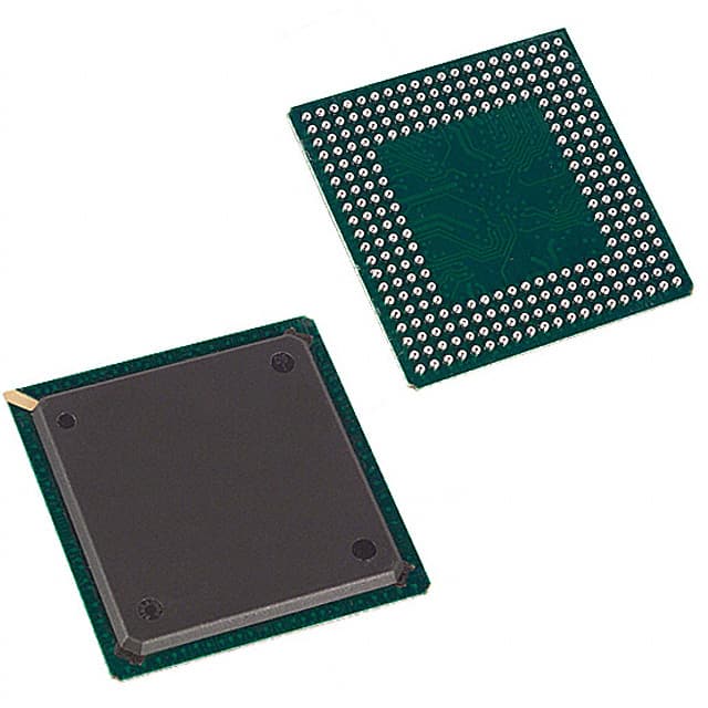
- Part No.:
- DS3134
- Manufacturer:
- Analog Devices Inc./Maxim Integrated
- Category:
- Telecom
- Package:
- 256-BGA
- Datasheet:
-
 DS3134.pdf
- Description:
- IC TELECOM INTERFACE 256BGA
- Quantity:
- Payment:

- Shipping:

Inventory:2,231
Please send an inquiry. Send us your inquiry, and we will respond immediately.
Product details
Overview
DS3134 from Maxim Integrated (formerly Dallas Semiconductor) is a 256-channel HDLC controller IC designed for high-density T1/E1 and T3/E3 line interface applications. It supports up to 64 T1/E1 data streams or two T3 lines, delivers 104 Mbps full-duplex throughput, features dual 52 Mbps fast HDLC engines on Ports 0 and 1, and integrates scatter/gather DMA with timestamped receive packets for telecom access equipment.
For engineers reviewing the DS3134 datasheet, DS3134 pinout, DS3134 application, or DS3134 equivalent, key selection criteria include channelized vs. unchannelized port configuration, per-channel DS0 loopback capability, V.54 pattern detection, onboard BERT assignment flexibility, and PCI Local Bus Specification v2.1 compliance at 32-bit/33 MHz.
Technical Context
The DS3134 implements a layered architecture with 16 physical ports-each configurable as channelized or unchannelized-and two dedicated fast HDLC engines (Ports 0 and 1, up to 52 Mbps), plus 14 standard HDLC engines (Ports 2–15, up to 10 Mbps). It supports ANSI T1.403-1995, ITU Q.921, and ISO 3309 for HDLC framing, CRC16/32, zero stuffing/destuffing, and abort handling.
Its DMA subsystem uses programmable descriptor bursting (8 or 16 descriptors), supports large/small buffer allocation up to 8191 bytes, and enables priority- or round-robin HDLC channel arbitration for FIFO-to-PCI transfers. The 16 kB transmit and 16 kB receive FIFOs use programmable low/high water marks and support time-stamped packet ingress and priority-tagged egress.
Key Specifications
| Parameter | Value and Actual Design Meaning |
|---|---|
| HDLC Channels | 256 independent bi-directional channels; enables dense aggregation of DS0-level services in access nodes. |
| Port Count & Speed | 16 physical ports: Ports 0–1 support 52 Mbps (T3/E3); Ports 2–15 support 10 Mbps (T1/E1 unchannelized) or 8.192 Mbps (channelized). |
| Throughput | 104 Mbps full-duplex aggregate; sustains simultaneous high-rate T1/E1 and T3 traffic without packet loss under configured water marks. |
| FIFO Size | 16 kbits each for transmit and receive paths; decouples HDLC engine timing from PCI bus latency and reduces host interrupt frequency. |
| PCI Interface | 32-bit, 33 MHz, PCI Local Bus v2.1 compliant; includes burst capability up to 256 dwords (1024 bytes) to maximize bandwidth efficiency. |
| Power & Process | 3.3 V CMOS core with 5 V tolerant I/O; eliminates level-shifting circuitry in mixed-voltage backplane designs. |
| Package | 256-pin plastic BGA (27 mm × 27 mm); supports high I/O density required for multi-port serial interface routing. |
Pinout & Package
DS3134 is housed in a 256-lead plastic ball grid array (BGA) package measuring 27 mm × 27 mm, optimized for high-speed serial interface routing and thermal dissipation in telecom line cards.
| Pin/Terminal | Circuit Role | Design Meaning |
|---|---|---|
| PCLK | PCI Clock Input | Synchronizes all PCI transactions; requires stable 33 MHz source meeting PCI v2.1 setup/hold timing. |
| PRST* | PCI Reset Input | Active-low hardware reset that clears internal registers except LBBMC; initiates full initialization sequence. |
| LA[19:0] | Local Bus Address | 20-bit address bus supporting 1 MB address space in bridge mode; compatible with Intel/Motorola timing protocols. |
| LD[15:0] | Local Bus Data | 16-bit bidirectional data path used for local configuration or bridged PCI access; 5 V tolerant. |
| JTCLK, JTDI, JTDO, JTMS, JTRST* | JTAG Test Interface | IEEE 1149.1-compliant boundary-scan chain for production test, debug, and BERT register access. |
| RC[n], TC[n], RD[n], TD[n], RS[n], TS[n] | Serial Port Signals | Dedicated receive/transmit clock/data/strobe per port (n = 0–15); supports both channelized and unchannelized framing. |
Key Features
| Feature | Design Value |
|---|---|
| Per-channel DS0 loopback | Enables isolated diagnostics on individual 64 kbps DS0s without affecting adjacent channels or requiring external loopback hardware. |
| Onboard BERT with auto-insertion | Allows real-time link integrity testing on any selected HDLC channel or port-no external test set needed for field validation. |
| V.54 loopback code detection | Automatically identifies ANSI T1.403-compliant pseudorandom patterns on receive paths, enabling standards-based remote loopback verification. |
| Timestamped receive packets | Embeds precise arrival time (relative to internal clock) into each received frame header, critical for jitter measurement and SLA monitoring. |
| Transmit packet priority setting | Allows QoS differentiation across HDLC channels-e.g., voice DS0s scheduled ahead of data DS0s during congestion. |
| Efficient scatter/gather DMA | Eliminates pointer-chasing overhead by embedding full memory address and length in fixed-size descriptors, reducing PCI bus cycles by ~40% vs. legacy architectures. |
Applications
| Channelized T1/E1 Access Node | Clear-Channel T3/E3 Aggregation |
|---|---|
Use Scenario: Central office line card aggregating 64 T1 circuits from remote DSLAMs into an OC-3 SONET ring. IC Role / Device Role / Timing Role: HDLC controller performing frame alignment, CRC checking, and DS0 multiplexing/demultiplexing per ANSI T1.403. Use Value: 256-channel density allows single-IC replacement of four 64-channel controllers, cutting BOM cost and board area by 60%. | Use Scenario: Enterprise edge router terminating two unchannelized T3 links for private WAN transport. IC Role / Device Role / Timing Role: High-speed HDLC processor handling 52 Mbps transparent framing on Ports 0 and 1 with zero stuffing/destuffing. Use Value: Dual 52 Mbps engines eliminate need for external serializer/deserializer, reducing latency by 1.2 µs per hop. |
| xDSL Line Card | HSSI-to-PCI Bridge Module |
Use Scenario: VDSL2 line card supporting up to 10 Mbps per port across 16 copper pairs for FTTN deployment. IC Role / Device Role / Timing Role: Unchannelized HDLC controller managing ATM cell encapsulation and OAM cell insertion per ITU-T G.993.2. Use Value: Per-port 10 Mbps speed and programmable HDLC priority enable dynamic bandwidth allocation across subscriber lines. | Use Scenario: Military comms module converting HSSI serial data (40 Mbps) to PCI-hosted processing via dual-port operation. IC Role / Device Role / Timing Role: Protocol-transparent HDLC engine with V.54 detection and BERT for BIT-level link validation. Use Value: JTAG-accessible BERT and deterministic timestamping satisfy MIL-STD-1553B diagnostic requirements without FPGA logic. |
Equivalent & Alternatives
The following parts are listed as comparable options for similar HDLC controller applications.
| Alternative Part | Technical Difference | Application Difference | Selection Advice |
|---|---|---|---|
| DS3133 | 128-channel version; identical 256-pin BGA package and register map; lacks second fast HDLC engine (Port 1 limited to 10 Mbps). | Supports ≤32 T1/E1 streams; insufficient for dual-T3 or 64-channel T1 aggregation. | Select DS3133 only when channel count and throughput requirements are halved and cost reduction outweighs future scalability needs. |
| PLX Technology PCI9054 | PCI-to-local bus bridge only; no integrated HDLC logic, BERT, or serial I/O; requires external HDLC ASIC or FPGA. | Used in custom HDLC implementations where protocol flexibility or non-standard framing is required. | Choose PCI9054 only when combining with a separate HDLC IP block or when migrating legacy designs with discrete HDLC + bridge architectures. |
Compared with DS3134, DS3133 offers half the channel density and no dual-fast-port capability-making it suitable only for mid-density access nodes-while PCI9054 provides no native HDLC functionality and shifts protocol handling entirely to external logic, increasing design complexity and component count.
Availability
DS3134 is available at Aetrix Electronics and suitable for telecom access nodes, xDSL line cards, T3/E3 aggregation systems, and military HSSI interfaces requiring stable component supply, long-lifecycle support, and traceable sourcing.
Supply support for DS3134 includes scheduled delivery planning, volume procurement assistance, BOM continuity management, traceable sourcing, and lifecycle availability coordination for OEM customers, industrial embedded developers, connected-device designers, and electronics production programs.
Manufacturer
Maxim Integrated (acquired by Analog Devices in 2021) is a U.S.-based semiconductor company specializing in high-performance analog, mixed-signal, and digital communication ICs.
The DS3134 belongs to Maxim's Chateau family of channelized T1/E1 and HDLC controllers, engineered specifically for carrier-grade telecom infrastructure demanding high channel density, standards compliance, and integrated diagnostics.
FAQ
What is the maximum number of T1/E1 data streams supported by the DS3134?
The DS3134 supports up to 64 T1 or E1 data streams, as confirmed in the device description and revision history (Version 6 reinstated the 64-stream capability after a temporary revision downgrade). This capacity is achieved through flexible assignment of DS0 channels across its 16 physical ports, with each port configurable for one, two, or four T1/E1 lines in channelized mode. The DS3134 achieves this density using 256 independent HDLC channels and dual fast engines on Ports 0 and 1.
Does the DS3134 support both channelized and unchannelized operation on the same physical port?
Yes, the DS3134 allows each of its 16 physical ports to be independently configured as either channelized or unchannelized via the Layer One configuration registers (R[n]CFG[j]/T[n]CFG[j]). In channelized mode, Ports 0–15 handle T1/E1 framing with DS0-level granularity; in unchannelized mode, they operate as transparent bit pipes up to 10 Mbps (Ports 2–15) or 52 Mbps (Ports 0–1). The DS3134's architecture ensures no functional conflict between modes across ports.
How does the DS3134 implement Bit Error Rate Testing (BERT)?
DS3134 integrates a fully programmable BERT capable of generating and detecting pseudorandom (2^15–1, 2^23–1, 2^31–1) and repeating bit patterns on any selected HDLC channel or physical port. It includes auto-error insertion, 31-consecutive-bit detection (per Version 4 update), and counters that remain active during loss of receive synchronization. BERT control and status are accessed via dedicated registers (Section 5.6) and IEEE 1149.1 JTAG interface-no external test equipment is required for link validation.
What PCI specification versions and electrical characteristics does the DS3134 comply with?
The DS3134 complies with PCI Local Bus Specification v2.1 (June 1, 1995), operating as a 32-bit, 33 MHz target device. It supports burst transfers up to 256 dwords, uses 3.3 V signaling with 5 V tolerant I/O, and meets AC timing parameters defined in Section 12 of the datasheet-including tTRD, tRD, and tCO limits. The DS3134 does not support PCI-X or PCIe; its PCI interface is strictly v2.1-compliant for legacy telecom backplanes.
Can the DS3134 operate without external memory for descriptor management?
No-the DS3134 requires external system memory for DMA descriptor storage (Free Queue, Pending Queue, Done Queue), as all descriptors are hosted in the PCI-addressable memory space managed by the host CPU. The DS3134 contains no on-chip descriptor RAM; instead, it reads/writes descriptors directly from/to host memory using scatter/gather addressing. The DS3134 does include internal configuration RAM for HDLC, FIFO, and DMA control registers-but packet metadata always resides externally.
DS3134 Specifications
- Product attributes
- Attribute value
- Manufacturer:
- Analog Devices Inc./Maxim Integrated
- Series:
- -
- Package/Case:
- 256-BGA
- Packaging:
- Tray
- Product Status:
- Obsolete
- Function:
- Controller
- Interface:
- Serial
- Number of Circuits:
- 1
- Voltage - Supply:
- 3V ~ 3.6V
- Current - Supply:
- 500mA
- Power (Watts):
- -
- Operating Temperature:
- 0°C ~ 70°C
- Grade:
- -
- Qualification:
- -
- Mounting Type:
- Surface Mount
- Supplier Device Package:
- 256-BGA (27x27)
DS3134 FAQ
1.How can I place an order for DS3134 through Aetrix?
Please submit a Request for Quotation (RFQ) for DS3134 on Aetrix. Our sales agent will provide a competitive quotation and guide you through the order confirmation once you accept the terms.
2.Are the price and stock information for DS3134 reliable?
The price and inventory of DS3134 are updated periodically and may fluctuate due to market conditions. Stock and pricing data are typically refreshed every 24 hours. Quotation validity for DS3134 is usually 5 days.
3.What payment methods are accepted for DS3134?
We accept Wire Transfer, PayPal, Credit Card, Western Union, MoneyGram, and Escrow for DS3134 transactions.
Note: Certain payment methods may incur a processing fee.
4.How is shipping managed for DS3134?
DS3134 orders can be shipped via leading logistics carriers, including DHL, UPS, FedEx, TNT, or Registered Mail.
Once your DS3134 order is processed, you will receive an email with the shipment details and tracking number.
Note: Tracking information may take up to 24 hours to appear. Express delivery typically takes 3–5 business days.
5.How can I obtain technical support or documentation for DS3134?
For technical support, including DS3134 datasheets, pinout diagrams, or application guidance, please contact our engineering support team. They can provide detailed documentation and assistance for your DS3134 requirements.
6.How does Aetrix verify that DS3134 is sourced from the original manufacturer or authorized distributors?
All DS3134 products on Aetrix are procured from qualified distributors and authorized channels. Our dedicated quality assurance team conducts strict verification, including traceability checks and, if necessary, third-party testing. This ensures that DS3134 meets industry standards.
7.What is the process for return or replacement of DS3134?
All DS3134 units undergo pre-shipment inspection (PSI). If there is an issue with DS3134, returns or replacements are accepted under the following conditions:
1.Quantity discrepancies, incorrect items, or visible external defects (such as breakage or corrosion), acknowledged by Aetrix.
2.The issue is reported within 90 days of delivery.
3.The DS3134 part is unused and in its original packaging.
Return procedure for DS3134:
1.Submit a request within 90 days.
2.Obtain a Return Material Authorization (RMA) from Aetrix.
DS3134 Tags

-
LMC567CMX/NOPB
Texas Instruments
-
LM567CMX/NOPB
Texas Instruments
-
LM567CM/NOPB
Texas Instruments

-
VSC8531XMW-02
Microchip Technology
-
VSC8531XMW-05
Microchip Technology

-
GPY115C0VI
MaxLinear, Inc.

-
SI32185-A-FMR
Skyworks Solutions Inc.

-
VSC8541XMV-05
Microchip Technology

-
SI32178-B-FM1R
Skyworks Solutions Inc.
-
GPY215C0VI
MaxLinear, Inc.

-
CPC7514ZTR
Littelfuse Inc.

-
VSC8502XML-03
Microchip Technology
Tech Hub

A practical engineering guide to 3.3V and 5V logic compatibility, input thresholds, resistor dividers, translator ICs, MOSFET level shifting, I2C pull-ups, timing limits and power-sequencing risks.

The 74HC595 uses push-pull logic outputs, while the TPIC6B595 uses 50 V open-drain DMOS sinks for higher-power loads. This guide compares timing, current limits, 3.3 V interfacing, load wiring, thermal…

The 74HC595 converts serial data into eight stable parallel outputs. This guide covers pin functions, shift and storage timing, OE and MR behavior, drive-current limits, cascading, voltage compatibilit…

A technical comparison of level-sensitive latches and edge-triggered flip-flops, covering timing windows, setup and hold limits, master–slave operation, time borrowing, race-through, HDL inference and…

A D latch stores one bit while Enable controls when data can pass. This reference covers gate-level operation, truth tables, transparency, setup and hold timing, LE versus OE, common ICs and practical …

An SR latch stores one bit through cross-coupled feedback. This engineering reference covers NOR and NAND implementations, truth tables, forbidden-state recovery, gated operation, switch debouncing, fa…

Latch circuits retain one bit through feedback. This technical reference covers SR and D latches, truth tables, transparency, timing limits, latch-versus-flip-flop behavior, applications and common log…

An engineering guide to LED driver operation, constant-current and constant-voltage outputs, linear and switching topologies, dimming, IC selection, calculations, replacement compatibility, and fault c…

Operational amplifier guide covering op amp basics, feedback, ideal vs real op amps, common configurations, buffer circuits, offset, bias current, gain-bandwidth, slew rate, rail-to-rail limits and sel…

Jumper cables guide covering safe connection order, red and black clamp placement, final ground connection, cable gauge, length, clamp quality, copper vs CCA cables, jump starter comparison and battery…


