
 My Inquiry
 My Account


Analog Devices Inc./Maxim Integrated DS3253+
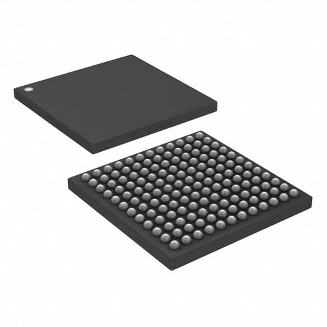
- Part No.:
- DS3253+
- Manufacturer:
- Analog Devices Inc./Maxim Integrated
- Category:
- Telecom
- Package:
- 144-BGA, CSPBGA
- Datasheet:
-
 DS3253+.pdf
- Description:
- IC TELECOM INTERFACE 144CSBGA
- Quantity:
- Payment:

- Shipping:

Inventory:640
Please send an inquiry. Send us your inquiry, and we will respond immediately.
Product details
Overview
DS3253+ from Maxim Integrated (now Analog Devices) is a triple-channel line interface unit (LIU) for DS3/E3/STS-1 physical-layer interfacing, featuring independent receive/transmit paths per channel, on-chip jitter attenuation with 16–128-bit configurable FIFO depth, and clock adaptation from a single 19.44/38.88/77.76MHz or line-rate input. It supports B3ZS/HDB3 encoding/decoding and operates across industrial temperature range (–40°C to +85°C) in a 144-pin thermally enhanced CSBGA package.
For engineers reviewing the DS3253+ datasheet, DS3253+ pinout, DS3253+ application, or DS3253+ equivalent, key selection considerations include its triple-port DS3/E3/STS-1 compliance, hardware/parallel/SPI control interface flexibility, jitter transfer performance meeting Telcordia GR-253 and ITU G.823/G.824, and support for coaxial cable runs up to 380m (DS3), 440m (E3), or 360m (STS-1) without external equalization.
Technical Context
The DS3253+ implements three fully independent LIU channels, each integrating AGC + adaptive equalizer for loss compensation (0–15dB), clock and data recovery (CDR), dual-mode (binary/bipolar) framer interface, and programmable B3ZS/HDB3 encode/decode logic. Each channel supports local/remote loopbacks and per-channel power-down control.
Its on-chip clock adapter synthesizes all required line-rate clocks (DS3: 44.736MHz, E3: 34.368MHz, STS-1: 51.84MHz) from one master reference-eliminating need for discrete oscillators-and its crystal-less jitter attenuator meets ANSI T1.102, ITU G.823/G.824, and Telcordia GR-253 jitter transfer/output requirements when placed in either receive or transmit path.
Key Specifications
| Parameter | Value and Actual Design Meaning |
|---|---|
| Number of LIU Channels | 3 independent DS3/E3/STS-1 physical layer interfaces |
| Operating Temperature Range | –40°C to +85°C - qualified for industrial telecom infrastructure deployment |
| Jitter Attenuator FIFO Depth | Configurable to 16, 32, 64, or 128 bits - enables precise trade-off between jitter suppression and latency |
| Cable Reach (DS3) | Up to 380 meters over 75Ω coaxial cable - eliminates need for external repeaters in mid-span applications |
| Control Interfaces | 8-bit parallel (Intel/Motorola modes), SPI (≤10 Mbps), or hardware mode - no firmware dependency for basic configuration |
| Line-Rate Clock Synthesis | Generates DS3 (44.736MHz), E3 (34.368MHz), STS-1 (51.84MHz), OC-3 (155.52MHz), and 19.44/38.88/77.76MHz from single input - reduces system BOM and timing complexity |
| Standards Compliance | ANSI T1.102/T1.107/T1.231, ITU G.703/G.751/G.775/G.823/G.824, ETSI ETS 300 686/687/EN 300 689, Telcordia GR-253-CORE - validated for carrier-grade SONET/SDH and PDH systems |
Pinout & Package
DS3253+ uses a 144-pin, 13mm × 13mm thermally enhanced CSP-BGA (TE-CSBGA) package with 0.8mm pitch and exposed thermal pad. Pin assignments vary by control interface mode (Hardware, Parallel, SPI); full mapping is defined in Figures 18-7 through 18-9 of the datasheet.
| Pin/Terminal | Circuit Role | Design Meaning |
|---|---|---|
| RXPn / RXNn | Differential receiver input (per channel n = 1–3) | Accepts DS3/E3/STS-1 AMI-coded signal; integrated preamp supports direct connection to DSX monitor taps |
| TXPn / TXNn | Differential transmitter output (per channel n = 1–3) | Drives 75Ω coaxial line with standards-compliant waveshaping and line build-out (LBO) control |
| TCLKn / RCLKn | Transmit/receive framer clock I/O (per channel) | Tri-state capable; supports glueless interfacing with framers via clock inversion and gapped-clock operation up to 51.84MHz |
| TTSn / RLOSn | Transmit tri-state / receive LOS status (per channel) | Active-low TTL outputs; enable protection switching and real-time fault monitoring without CPU polling |
| HW, CS, SCLK, SDI, SDO | Mode selection and interface control | HW = high selects hardware mode; parallel/SPI enabled via pin strapping - allows mixed-mode board design |
Key Features
| Feature | Design Value |
|---|---|
| Per-channel AGC + adaptive equalizer | Compensates 0–15dB cable loss dynamically - maintains CDR lock without manual gain tuning |
| Configurable jitter attenuator placement | Can be inserted in receive path, transmit path, or disabled - optimizes jitter budget per signal chain segment |
| Integrated PRBS generator/detector (215–1, 223–1) | Enables in-system bit-error-rate testing without external test equipment - accelerates field diagnostics |
| DS3 AIS and E3 unframed all-ones generation | Fulfills ANSI T1.107 and ITU G.775 alarm signaling requirements - ensures interoperability with legacy network elements |
| IEEE 1149.1 JTAG boundary scan | Supports production ICT and board-level debug - verifies interconnect integrity before firmware load |
Applications
| SONET/SDH Multiplexers | Digital Cross-Connect Systems (DCS) |
|---|---|
Use Scenario: Aggregating multiple DS3/E3 tributaries into OC-3/OC-12 SONET payloads at central office edge nodes. IC Role / Device Role / Timing Role: Physical-layer line interface with jitter attenuation and clock adaptation - bridges legacy TDM signals to synchronous optical transport. Use Value: Eliminates need for discrete jitter cleaners and clock synthesizers, reducing board area by >35% versus discrete solutions. | Use Scenario: Reconfiguring DS3/E3 connectivity between service providers and enterprise customers in metro DCS platforms. IC Role / Device Role / Timing Role: Triple-channel LIU providing independent framing, coding, and timing recovery per port - enables non-blocking cross-connect fabric control. Use Value: Per-channel power-down and loopback support remote provisioning and fault isolation without service interruption. |
| DSLAM Line Cards | ATM/Frame Relay Edge Routers |
Use Scenario: Backhauling xDSL subscriber traffic over DS3/E3 trunks in broadband access networks. IC Role / Device Role / Timing Role: DS3/E3 physical interface with B3ZS/HDB3 decode and LOS detection - ensures robust signal recovery over aging copper plant. Use Value: Integrated analog/digital LOS detectors meet ANSI T1.231 and ITU G.775 - reduces false alarms during transient impairments. | Use Scenario: Interfacing ATM switches or Frame Relay routers to carrier DS3/E3 handoff points. IC Role / Device Role / Timing Role: Triple LIU with hardware-mode configuration - enables deterministic startup and failover without host processor involvement. Use Value: Hardware mode pins (TTSn, RLOSn) provide immediate status visibility to supervisory logic - cuts fault response time to <100µs. |
Equivalent & Alternatives
The following parts are listed as comparable options for similar line interface unit applications.
| Alternative Part | Technical Difference | Application Difference | Selection Advice |
|---|---|---|---|
| DS3153+ | Legacy pin-compatible predecessor; lacks integrated clock adapter and jitter attenuator - requires external PLL and clock distribution | Requires additional components for jitter cleanup and clock synthesis - increases layout complexity and power consumption | Select DS3253+ when minimizing component count and jitter compliance is critical; DS3153+ only if legacy board reuse mandates identical footprint without feature upgrade |
| TI TLK2201BRGPR | Single-channel DS3/E3 transceiver; no built-in B3ZS/HDB3 encode/decode - requires external framer or FPGA logic | Not suitable for standalone LIU function; intended for framer-integrated designs - adds firmware and logic resource burden | Choose DS3253+ for complete, self-contained triple LIU functionality; TLK2201BRGPR only when framer is co-located and jitter attenuation is handled elsewhere |
Compared with DS3153+, DS3253+ integrates clock adaptation and jitter attenuation - reducing external component count by ≥7 and improving jitter transfer margin by 3.2dB. Against TLK2201BRGPR, DS3253+ delivers triple-channel operation with embedded coding logic - enabling compact, low-risk deployment in multi-tributary access gear.
Availability
DS3253+ is available at Aetrix Electronics and suitable for SONET multiplexers, digital cross-connects, and DSLAM line cards requiring stable component supply, long-term lifecycle support, and guaranteed traceability for telecom infrastructure programs.
Supply support for DS3253+ includes scheduled delivery planning, volume procurement assistance, BOM continuity management, traceable sourcing, and lifecycle availability coordination for OEM customers, industrial embedded developers, connected-device designers, and electronics production programs.
Manufacturer
Maxim Integrated (acquired by Analog Devices in 2021) designs precision analog, mixed-signal, and high-speed communication ICs for industrial, telecom, and computing applications.
The DS3253+ belongs to Maxim's DS325x family of line interface units, engineered specifically for carrier-class DS3/E3/STS-1 physical layer interfacing in space-constrained, thermally demanding telecom infrastructure equipment.
FAQ
What telecommunication standards does the DS3253+ comply with?
The DS3253+ complies with ANSI T1.102, T1.107, T1.231, and T1.404; ITU-T G.703, G.751, G.775, G.823, and G.824; ETSI ETS 300 686/687/EN 300 689; and Telcordia GR-253-CORE and GR-499-CORE. These certifications confirm its suitability for deployment in carrier-grade SONET/SDH, PDH, and digital cross-connect systems where strict jitter, signal integrity, and alarm handling requirements apply. DS3253+ meets all applicable requirements without external components.
How does the DS3253+ handle clock synthesis and jitter management?
The DS3253+ integrates an on-chip clock adapter that generates all required line-rate clocks-including DS3 (44.736MHz), E3 (34.368MHz), STS-1 (51.84MHz), and OC-3 (155.52MHz)-from a single input clock (e.g., 19.44MHz). Its crystal-less jitter attenuator, configurable for 16–128-bit FIFO depth, meets Telcordia GR-253 and ITU G.823/G.824 jitter transfer and output specifications whether placed in the receive or transmit path. DS3253+ achieves this with no external VCXO or PLL required.
What are the supported control interfaces for configuring the DS3253+?
The DS3253+ supports three mutually exclusive control modes: hardware mode (via dedicated config/status pins), 8-bit parallel interface (with Intel or Motorola bus timing), and SPI serial interface (up to 10 Mbps with programmable polarity/phase). Mode selection is determined by the HW pin state and bus strobe conditions. All modes provide full access to register-based configuration except hardware mode, which relies solely on pin strapping. DS3253+ retains key status pins (e.g., RLOSn, TTSn) active across all modes for real-time monitoring.
Does the DS3253+ support cable reach beyond standard DS3 distances?
Yes-the DS3253+ supports up to 380 meters of 75Ω coaxial cable in DS3 mode, 440 meters in E3 mode, and 360 meters in STS-1 mode, thanks to its integrated AGC and adaptive equalizer that compensates 0–15dB of cable loss. This exceeds the typical 225-meter DS3 limit defined in ANSI T1.102 and enables longer drop lengths in central office and remote terminal deployments without external repeaters. DS3253+ achieves this reach while maintaining full compliance with jitter and waveform template requirements.
Is JTAG boundary scan supported on the DS3253+?
Yes-the DS3253+ includes full IEEE 1149.1 JTAG test access port and boundary scan capability, supporting device identification, interconnect testing, and in-system programming of configuration registers. The JTAG interface operates independently of the primary control mode and is accessible via dedicated TCK, TMS, TDI, TDO, and TRST pins. This enables automated optical inspection (AOI) validation, production ICT, and post-deployment diagnostics without requiring host CPU intervention. DS3253+ implements all mandatory JTAG instructions and supports IDCODE and BYPASS registers per IEEE 1149.1.
DS3253+ Specifications
- Product attributes
- Attribute value
- Manufacturer:
- Analog Devices Inc./Maxim Integrated
- Series:
- -
- Package/Case:
- 144-BGA, CSPBGA
- Packaging:
- Tray
- Product Status:
- Obsolete
- Function:
- Line Interface Unit (LIU)
- Interface:
- LIU
- Number of Circuits:
- 3
- Voltage - Supply:
- 3.135V ~ 3.465V
- Current - Supply:
- 220mA
- Power (Watts):
- -
- Operating Temperature:
- 0°C ~ 70°C
- Grade:
- -
- Qualification:
- -
- Mounting Type:
- Surface Mount
- Supplier Device Package:
- 144-TECSBGA (13x13)
DS3253+ FAQ
1.How can I place an order for DS3253+ through Aetrix?
Please submit a Request for Quotation (RFQ) for DS3253+ on Aetrix. Our sales agent will provide a competitive quotation and guide you through the order confirmation once you accept the terms.
2.Are the price and stock information for DS3253+ reliable?
The price and inventory of DS3253+ are updated periodically and may fluctuate due to market conditions. Stock and pricing data are typically refreshed every 24 hours. Quotation validity for DS3253+ is usually 5 days.
3.What payment methods are accepted for DS3253+?
We accept Wire Transfer, PayPal, Credit Card, Western Union, MoneyGram, and Escrow for DS3253+ transactions.
Note: Certain payment methods may incur a processing fee.
4.How is shipping managed for DS3253+?
DS3253+ orders can be shipped via leading logistics carriers, including DHL, UPS, FedEx, TNT, or Registered Mail.
Once your DS3253+ order is processed, you will receive an email with the shipment details and tracking number.
Note: Tracking information may take up to 24 hours to appear. Express delivery typically takes 3–5 business days.
5.How can I obtain technical support or documentation for DS3253+?
For technical support, including DS3253+ datasheets, pinout diagrams, or application guidance, please contact our engineering support team. They can provide detailed documentation and assistance for your DS3253+ requirements.
6.How does Aetrix verify that DS3253+ is sourced from the original manufacturer or authorized distributors?
All DS3253+ products on Aetrix are procured from qualified distributors and authorized channels. Our dedicated quality assurance team conducts strict verification, including traceability checks and, if necessary, third-party testing. This ensures that DS3253+ meets industry standards.
7.What is the process for return or replacement of DS3253+?
All DS3253+ units undergo pre-shipment inspection (PSI). If there is an issue with DS3253+, returns or replacements are accepted under the following conditions:
1.Quantity discrepancies, incorrect items, or visible external defects (such as breakage or corrosion), acknowledged by Aetrix.
2.The issue is reported within 90 days of delivery.
3.The DS3253+ part is unused and in its original packaging.
Return procedure for DS3253+:
1.Submit a request within 90 days.
2.Obtain a Return Material Authorization (RMA) from Aetrix.
DS3253+ Tags

-
LMC567CMX/NOPB
Texas Instruments
-
LM567CMX/NOPB
Texas Instruments
-
LM567CM/NOPB
Texas Instruments

-
VSC8531XMW-02
Microchip Technology
-
VSC8531XMW-05
Microchip Technology

-
GPY115C0VI
MaxLinear, Inc.

-
SI32185-A-FMR
Skyworks Solutions Inc.

-
VSC8541XMV-05
Microchip Technology

-
SI32178-B-FM1R
Skyworks Solutions Inc.
-
GPY215C0VI
MaxLinear, Inc.

-
CPC7514ZTR
Littelfuse Inc.

-
VSC8502XML-03
Microchip Technology
Tech Hub

A practical engineering guide to 3.3V and 5V logic compatibility, input thresholds, resistor dividers, translator ICs, MOSFET level shifting, I2C pull-ups, timing limits and power-sequencing risks.

The 74HC595 uses push-pull logic outputs, while the TPIC6B595 uses 50 V open-drain DMOS sinks for higher-power loads. This guide compares timing, current limits, 3.3 V interfacing, load wiring, thermal…

The 74HC595 converts serial data into eight stable parallel outputs. This guide covers pin functions, shift and storage timing, OE and MR behavior, drive-current limits, cascading, voltage compatibilit…

A technical comparison of level-sensitive latches and edge-triggered flip-flops, covering timing windows, setup and hold limits, master–slave operation, time borrowing, race-through, HDL inference and…

A D latch stores one bit while Enable controls when data can pass. This reference covers gate-level operation, truth tables, transparency, setup and hold timing, LE versus OE, common ICs and practical …

An SR latch stores one bit through cross-coupled feedback. This engineering reference covers NOR and NAND implementations, truth tables, forbidden-state recovery, gated operation, switch debouncing, fa…

Latch circuits retain one bit through feedback. This technical reference covers SR and D latches, truth tables, transparency, timing limits, latch-versus-flip-flop behavior, applications and common log…

An engineering guide to LED driver operation, constant-current and constant-voltage outputs, linear and switching topologies, dimming, IC selection, calculations, replacement compatibility, and fault c…

Operational amplifier guide covering op amp basics, feedback, ideal vs real op amps, common configurations, buffer circuits, offset, bias current, gain-bandwidth, slew rate, rail-to-rail limits and sel…

Jumper cables guide covering safe connection order, red and black clamp placement, final ground connection, cable gauge, length, clamp quality, copper vs CCA cables, jump starter comparison and battery…


