
 My Inquiry
 My Account


Texas Instruments DS34RT5110SQ/NOPB
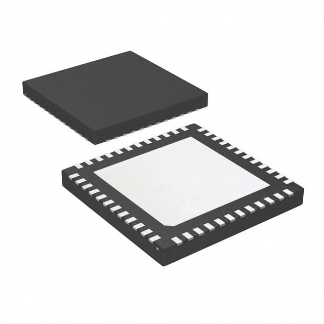
- Part No.:
- DS34RT5110SQ/NOPB
- Manufacturer:
- Texas Instruments
- Category:
- Video Processing
- Package:
- 48-WFQFN Exposed Pad
- Datasheet:
-
 DS34RT5110SQ/NOPB.pdf
- Description:
- IC VIDEO RETIMER 48WQFN
- Quantity:
- Payment:

- Shipping:

Inventory:3,398
Please send an inquiry. Send us your inquiry, and we will respond immediately.
Product details
Overview
DS34RT5110SQ/NOPB from Texas Instruments is a 10.2 Gbps HDMI/DVI retimer IC with integrated input equalization and output de-emphasis, supporting three TMDS data channels and one clock channel at up to 3.4 Gbps per channel. It features dedicated CDR per data channel, <0.10 UI total output jitter at 3.4 Gbps, and resistor-adjustable differential output voltage for AC/DC-coupled Cat5e/Cat6 or HDMI cable extension in video routing systems.
For engineers reviewing the DS34RT5110SQ/NOPB datasheet, DS34RT5110SQ/NOPB pinout, DS34RT5110SQ/NOPB application, or DS34RT5110SQ/NOPB equivalent, this device is selected for high-fidelity multi-hop HDMI signal regeneration, long-reach source/sink interface conditioning, and low-jitter clock-data recovery in professional AV distribution equipment requiring stable 3.3 V operation and WQFN-48 packaging.
Technical Context
The DS34RT5110SQ/NOPB implements independent CDRs per TMDS data channel, each digitally interpolating sampling clock edges from a shared high-performance PLL on the clock channel. Its equalizer supports eight programmable boost levels (0–27 dB) via EQ[2:0] pins, while output de-emphasis offers four selectable levels (0, −3, −6, −9 dB) via DE[1:0]. The PLL loop bandwidth scales with data rate (e.g., 2.25 MHz at 2.25 Gbps), enabling deterministic jitter suppression across 250 Mbps–3.4 Gbps.
Each channel uses CML I/O with on-chip 50 Ω input termination to VDD and open-collector outputs. Output differential voltage (VO) is set by external resistor on VOD_CRL pin (24 kΩ for DC-coupled, 12 kΩ for AC-coupled), delivering 800–1200 mVp-p. Signal Detect (SD) and LOCK status pins provide real-time channel health monitoring for system-level fault handling.
Key Specifications
| Parameter | Value and Actual Design Meaning |
|---|---|
| Max Data Rate | 3.4 Gbps per TMDS data channel; supports full 10.2 Gbps aggregate HDMI v1.3a / DVI v1.0 throughput. |
| Total Output Jitter | 0.10 UIp-p at 3.4 Gbps; ensures timing margin for downstream receivers in multi-hop cascades. |
| Input Equalization | 8 programmable levels (0–27 dB); compensates >25 m of 28 AWG HDMI cable loss at 2.25 Gbps. |
| Output De-Emphasis | 4 levels (0, −3, −6, −9 dB); optimizes driving capability for FR4 traces or extended Cat5e/Cat6 links. |
| Supply Voltage | 3.3 V ±5%; requires six 0.1 µF bypass capacitors across VDD pins for stable CML/CDR operation. |
| Operating Temperature | 0 °C to +70 °C; validated for commercial-grade AV equipment including matrix switches and extenders. |
| ESD Protection | >8 kV HBM; protects TMDS I/O against electrostatic discharge during board assembly and field service. |
Pinout & Package
DS34RT5110SQ/NOPB is housed in a 7 mm × 7 mm, 48-pin WQFN package (RHS0048A) with exposed thermal pad (DAP) tied to ground. Pin functions are validated per TI SNLS310G datasheet Rev. April 2013.
| Pin/Terminal | Circuit Role | Design Meaning |
|---|---|---|
| C_IN+, C_IN− | TMDS Clock Input | Differential CML inputs with internal 50 Ω termination to VDD; feed clock-channel PLL. |
| D_IN0+ to D_IN2− | TMDS Data Inputs | Three differential CML data input pairs; each connects to dedicated equalizer + CDR block. |
| C_OUT+, C_OUT− | TMDS Clock Output | Open-collector CML outputs; regenerated low-jitter clock for downstream data recovery. |
| D_OUT0+ to D_OUT2− | TMDS Data Outputs | Three open-collector CML data outputs; de-emphasized, retimed signals for cable extension. |
| EQ2–EQ0 | Equalization Control | LVCMOS inputs selecting 1 of 8 boost levels (0–27 dB); default = 000 (0 dB). |
| DE1–DE0 | De-Emphasis Control | LVCMOS inputs selecting 1 of 4 de-emphasis levels (0 to −9 dB); default = 00 (0 dB). |
| BYPASS, EN, MODE | Functional Mode Control | LVCMOS pins enabling retiming bypass (BYPASS), output driver enable (EN), and clock channel bypass (MODE). |
| SD, LOCK | Status Outputs | LVCMOS outputs indicating signal presence (SD) and PLL lock status (LOCK) for system supervision. |
| VOD_CRL, LFn, LFp | Analog Configuration | VOD_CRL sets output swing (24 kΩ/12 kΩ); LFn/LFp connect external RC loop filter for PLL stability. |
Key Features
| Feature | Design Value |
|---|---|
| Dedicated CDR per data channel | Enables independent jitter cleanup and latency control across all three TMDS lanes without inter-channel coupling. |
| Configurable receive equalization | Eight discrete boost settings (0–27 dB) allow precise compensation for varying cable loss profiles at 250 Mbps–3.4 Gbps. |
| Resistor-adjustable output voltage | VOD_CRL pin accepts 12 kΩ (AC-coupled) or 24 kΩ (DC-coupled) to ground, ensuring 1000 mVp-p VO compliance with HDMI sink requirements. |
| Multi-hop cascade support | Low jitter transfer (<0.09 UI at 2.25 Gbps) enables ≥3-device daisy chains without signal fidelity degradation in professional AV routing. |
| Integrated signal integrity monitoring | SD and LOCK pins provide real-time LVCMOS status flags for automatic power management and system diagnostics. |
Applications
| Video Matrix Switching | HDMI/DVI Repeater Extender |
|---|---|
Use Scenario: Centralized DVI/HDMI routing in security command centers with 16+ sources feeding multiple displays over 20 m CAT5e cables. IC Role / Device Role / Timing Role: DS34RT5110SQ/NOPB acts as a signal conditioner at both source and sink ports, equalizing incoming signals and regenerating clean TMDS outputs with sub-0.10 UI jitter. Use Value: Eliminates PCB trace-induced jitter and compensates for UTP skew, enabling reliable 1080p60 transmission across non-standard cabling without protocol violation. |
Use Scenario: Bi-directional HDMI extender box extending 1080p/48-bit color signals over 30 m of shielded twisted-pair cable between projector and media player. IC Role / Device Role / Timing Role: DS34RT5110SQ/NOPB serves as a repeater core, applying optimized EQ (0x06) and DE (−6 dB) to restore signal integrity after cable attenuation. Use Value: Extends reach beyond native HDMI limits while maintaining <0.10 UI jitter, avoiding pixel dropouts or audio sync errors in live presentation environments. |
| Multi-Hop Studio Distribution | Dual-Link DVI Repeater |
Use Scenario: Three-stage HDMI distribution in broadcast studios linking camera feeds through patch panels, processing units, and master monitors over 60 m total cable length. IC Role / Device Role / Timing Role: DS34RT5110SQ/NOPB deployed in cascade: first two stages use MODE = HIGH (clock bypass) to minimize jitter accumulation; final stage uses MODE = LOW for clock cleanup. Use Value: Achieves end-to-end jitter <0.12 UI across three hops-enabling stable 1080p/12-bit color delivery where single-hop solutions fail. |
Use Scenario: QXGA (2048×1536) display interface requiring dual-link DVI bandwidth, implemented using two synchronized DS34RT5110SQ/NOPB devices. IC Role / Device Role / Timing Role: Each DS34RT5110SQ/NOPB handles one DVI link (3 data + 1 clock), with matched EQ/DE settings and shared PLL reference for inter-link timing alignment. Use Value: Supports ultra-high-resolution digital signage and medical imaging displays with deterministic latency and no inter-pair skew amplification. |
Equivalent & Alternatives
The following parts are listed as comparable options for similar HDMI/DVI retimer applications.
| Alternative Part | Technical Difference | Application Difference | Selection Advice |
|---|---|---|---|
| TI DS34S400 | Single-channel 3.4 Gbps retimer; no integrated clock channel PLL; requires external clock source. | Suitable only for point-to-point extensions where clock regeneration is handled externally. | Select DS34S400 when system already provides low-jitter clock reference and only data-channel retiming is needed. |
| Maxim MAX3815 | 4-channel 1.65 Gbps retimer; max 0.15 UI jitter at 1.65 Gbps; no programmable de-emphasis; 0 °C to +85 °C range. | Limited to 1080i/720p; lacks HDMI v1.3a 10.2 Gbps support and multi-hop jitter performance. | Choose MAX3815 only for cost-sensitive legacy HD-SDI hybrid interfaces requiring industrial temperature range. |
Compared with DS34RT5110SQ/NOPB, DS34S400 reduces system BOM count where clock synthesis is centralized, while MAX3815 trades bandwidth and jitter performance for wider temperature tolerance-neither matches DS34RT5110SQ/NOPB's 10.2 Gbps aggregate throughput, per-channel CDR, or multi-hop signal fidelity.
Availability
DS34RT5110SQ/NOPB is available at Aetrix Electronics and suitable for HDMI matrix switching, multi-hop video extenders, broadcast studio distribution, and dual-link DVI repeaters requiring stable component supply and long-term lifecycle support.
Supply support for DS34RT5110SQ/NOPB includes scheduled delivery planning, volume procurement assistance, BOM continuity management, traceable sourcing, and lifecycle availability coordination for OEM customers, industrial embedded developers, connected-device designers, and electronics production programs.
Manufacturer
Texas Instruments is a global semiconductor leader specializing in analog, embedded processing, and connectivity technologies for industrial, automotive, and communications markets.
The DS34RT5110SQ/NOPB belongs to TI's Display Interface product line, engineered specifically for high-speed video signal integrity restoration in HDMI/DVI infrastructure-addressing cable loss, jitter accumulation, and timing margin constraints in professional AV systems.
FAQ
What is the maximum supported data rate per channel for DS34RT5110SQ/NOPB?
The DS34RT5110SQ/NOPB supports up to 3.4 Gbps per TMDS data channel, enabling full 10.2 Gbps aggregate throughput for HDMI v1.3a and DVI v1.0 applications including 1080p with 48-bit deep color. This rate is validated across the full operating temperature range (0 °C to +70 °C) and confirmed in TI's SNLS310G datasheet Section 6.5.
How does DS34RT5110SQ/NOPB handle jitter reduction in multi-hop configurations?
DS34RT5110SQ/NOPB reduces jitter accumulation in multi-hop setups via dedicated per-channel CDRs and a low-jitter PLL clock channel. Total output jitter remains ≤0.09 UI at 2.25 Gbps and ≤0.10 UI at 3.4 Gbps, allowing ≥3 devices to be cascaded without violating HDMI timing budgets-verified in TI application note SNLA207.
Can DS34RT5110SQ/NOPB be used with AC-coupled Cat6 cable, and what configuration is required?
Yes, DS34RT5110SQ/NOPB supports AC-coupled Cat6 extension. Configure VOD_CRL with 12 kΩ to ground for 1000 mVp-p output swing, add 50 Ω pull-up resistors near source outputs, and place 622 Ω pull-down resistors at sink inputs to set common-mode voltage to 3.05 V-details in SNLS310G Section 9.3.
What is the function of the MODE pin on DS34RT5110SQ/NOPB, and when should it be asserted HIGH?
The MODE pin bypasses the clock channel PLL. Assert MODE = HIGH in intermediate hops of multi-hop systems to prevent jitter accumulation from successive PLLs; retain MODE = LOW in the final hop to regenerate a clean, low-jitter clock for sink devices-as specified in SNLS310G Figure 9 and Section 8.4.
Does DS34RT5110SQ/NOPB require external loop filter components, and if so, what values are recommended?
Yes, DS34RT5110SQ/NOPB requires an external RC loop filter between LFn and LFp pins. TI specifies a 3.3 kΩ ±5% resistor in series with a 2.2 nF ±5% capacitor (SNLS310G Section 8.1). This network stabilizes the clock-channel PLL and ensures optimal jitter performance across all supported data rates.
DS34RT5110SQ/NOPB Specifications
- Product attributes
- Attribute value
- Manufacturer:
- Texas Instruments
- Series:
- -
- Package/Case:
- 48-WFQFN Exposed Pad
- Packaging:
- Tape & Reel (TR)
- Product Status:
- Not For New Designs
- Function:
- Retimer
- Applications:
- -
- Standards:
- -
- Control Interface:
- -
- Voltage - Supply:
- -
- Mounting Type:
- Surface Mount
- Grade:
- -
- Qualification:
- -
- Supplier Device Package:
- 48-WQFN (7x7)
DS34RT5110SQ/NOPB FAQ
1.How can I place an order for DS34RT5110SQ/NOPB through Aetrix?
Please submit a Request for Quotation (RFQ) for DS34RT5110SQ/NOPB on Aetrix. Our sales agent will provide a competitive quotation and guide you through the order confirmation once you accept the terms.
2.Are the price and stock information for DS34RT5110SQ/NOPB reliable?
The price and inventory of DS34RT5110SQ/NOPB are updated periodically and may fluctuate due to market conditions. Stock and pricing data are typically refreshed every 24 hours. Quotation validity for DS34RT5110SQ/NOPB is usually 5 days.
3.What payment methods are accepted for DS34RT5110SQ/NOPB?
We accept Wire Transfer, PayPal, Credit Card, Western Union, MoneyGram, and Escrow for DS34RT5110SQ/NOPB transactions.
Note: Certain payment methods may incur a processing fee.
4.How is shipping managed for DS34RT5110SQ/NOPB?
DS34RT5110SQ/NOPB orders can be shipped via leading logistics carriers, including DHL, UPS, FedEx, TNT, or Registered Mail.
Once your DS34RT5110SQ/NOPB order is processed, you will receive an email with the shipment details and tracking number.
Note: Tracking information may take up to 24 hours to appear. Express delivery typically takes 3–5 business days.
5.How can I obtain technical support or documentation for DS34RT5110SQ/NOPB?
For technical support, including DS34RT5110SQ/NOPB datasheets, pinout diagrams, or application guidance, please contact our engineering support team. They can provide detailed documentation and assistance for your DS34RT5110SQ/NOPB requirements.
6.How does Aetrix verify that DS34RT5110SQ/NOPB is sourced from the original manufacturer or authorized distributors?
All DS34RT5110SQ/NOPB products on Aetrix are procured from qualified distributors and authorized channels. Our dedicated quality assurance team conducts strict verification, including traceability checks and, if necessary, third-party testing. This ensures that DS34RT5110SQ/NOPB meets industry standards.
7.What is the process for return or replacement of DS34RT5110SQ/NOPB?
All DS34RT5110SQ/NOPB units undergo pre-shipment inspection (PSI). If there is an issue with DS34RT5110SQ/NOPB, returns or replacements are accepted under the following conditions:
1.Quantity discrepancies, incorrect items, or visible external defects (such as breakage or corrosion), acknowledged by Aetrix.
2.The issue is reported within 90 days of delivery.
3.The DS34RT5110SQ/NOPB part is unused and in its original packaging.
Return procedure for DS34RT5110SQ/NOPB:
1.Submit a request within 90 days.
2.Obtain a Return Material Authorization (RMA) from Aetrix.
DS34RT5110SQ/NOPB Tags

-
HDMI2C1-6C1
STMicroelectronics

-
ADA4430-1YKSZ-R7
Analog Devices Inc.

-
LM1881MX/NOPB
Texas Instruments

-
SN75DP130SSRGZR
Texas Instruments

-
EQCO30T5.2
Microchip Technology

-
LMH1980MM/NOPB
Texas Instruments
-
EQCO30R5.D
Microchip Technology

-
SII9022ACNU
Lattice Semiconductor Corporation
-
SN65DP159RGZR
Texas Instruments

-
SN65DP159RSBR
Texas Instruments

-
SN65DP141RLJR
Texas Instruments

-
LMH0303SQ/NOPB
Texas Instruments
Tech Hub

A practical engineering guide to 3.3V and 5V logic compatibility, input thresholds, resistor dividers, translator ICs, MOSFET level shifting, I2C pull-ups, timing limits and power-sequencing risks.

The 74HC595 uses push-pull logic outputs, while the TPIC6B595 uses 50 V open-drain DMOS sinks for higher-power loads. This guide compares timing, current limits, 3.3 V interfacing, load wiring, thermal…

The 74HC595 converts serial data into eight stable parallel outputs. This guide covers pin functions, shift and storage timing, OE and MR behavior, drive-current limits, cascading, voltage compatibilit…

A technical comparison of level-sensitive latches and edge-triggered flip-flops, covering timing windows, setup and hold limits, master–slave operation, time borrowing, race-through, HDL inference and…

A D latch stores one bit while Enable controls when data can pass. This reference covers gate-level operation, truth tables, transparency, setup and hold timing, LE versus OE, common ICs and practical …

An SR latch stores one bit through cross-coupled feedback. This engineering reference covers NOR and NAND implementations, truth tables, forbidden-state recovery, gated operation, switch debouncing, fa…

Latch circuits retain one bit through feedback. This technical reference covers SR and D latches, truth tables, transparency, timing limits, latch-versus-flip-flop behavior, applications and common log…

An engineering guide to LED driver operation, constant-current and constant-voltage outputs, linear and switching topologies, dimming, IC selection, calculations, replacement compatibility, and fault c…

Operational amplifier guide covering op amp basics, feedback, ideal vs real op amps, common configurations, buffer circuits, offset, bias current, gain-bandwidth, slew rate, rail-to-rail limits and sel…

Jumper cables guide covering safe connection order, red and black clamp placement, final ground connection, cable gauge, length, clamp quality, copper vs CCA cables, jump starter comparison and battery…


