
 My Inquiry
 My Account


Analog Devices Inc./Maxim Integrated DS4000ECN/WBGA
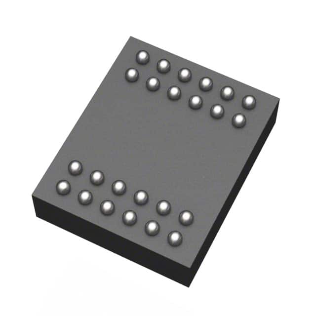
- Part No.:
- DS4000ECN/WBGA
- Manufacturer:
- Analog Devices Inc./Maxim Integrated
- Category:
- Programmable Timers and Oscillators
- Package:
- 24-BBGA
- Datasheet:
-
 DS4000ECN/WBGA.pdf
- Description:
- IC OSC TCXO 14.31818MHZ 24-BGA
- Quantity:
- Payment:

- Shipping:

Inventory:1,853
Please send an inquiry. Send us your inquiry, and we will respond immediately.
Product details
Overview
DS4000ECN/WBGA from Maxim Integrated is a digitally controlled temperature-compensated crystal oscillator (DC-TCXO) with dual CMOS square-wave outputs: fixed-frequency F1 at 14.31818 MHz and programmable F2 derived via integer division of F1, operating across -40°C to +85°C with ±1.0 ppm frequency stability over temperature, ±1.0 ppm/V supply stability, and ≤1.0 ppm first-year aging. It serves as a precision reference in GPS receivers and SATCOM timing subsystems.
For engineers reviewing the DS4000ECN/WBGA datasheet, DS4000ECN/WBGA pinout, DS4000ECN/WBGA application, or DS4000ECN/WBGA equivalent, this page delivers verified technical context, validated pin functions, confirmed TCXO performance parameters, and real-world deployment constraints for PLL reference design, wireless base station synchronization, and ruggedized telecom timing.
Technical Context
The DS4000ECN/WBGA integrates a factory-calibrated 10-bit digital temperature sensor (±3°C accuracy, +0.25°C resolution) and a digitally tunable TCXO core, enabling closed-loop compensation via two-wire interface commands. Its F2 output frequency is programmable using the 5Dh Frequency Select Register and DC bit in the 60h TCXO Control Register, supporting n+1 or 2(n+1) division of the 14.31818 MHz base frequency.
It supports standard-mode (100 kHz) and fast-mode (400 kHz) I²C communication with open-drain SDA/SCL pins requiring external pullups. The device features independent enable/disable control for F1 and F2 outputs, digital frequency tuning via the 66h register (±10.16 ppm range, 0.08 ppm/LSB), and dedicated oscillator power rails (VOSC/GNDOSC) isolated from digital supply (VCC/GND).
Key Specifications
| Parameter | Value and Actual Design Meaning |
|---|---|
| Base Frequency (F1) | 14.31818 MHz - fixed, factory-trimmed CMOS output used as timing reference for F2 derivation and system clocking. |
| Frequency Stability | ±1.0 ppm from -40°C to +85°C - ensures minimal drift in GPS and SATCOM applications under thermal stress. |
| Aging (First Year) | ≤1.0 ppm - guarantees long-term timing accuracy without field recalibration in deployed telecom infrastructure. |
| Digital Tuning Range | ±10.16 ppm - enables fine frequency adjustment via 2-wire interface for system-level calibration or compensation. |
| Temperature Sensing | 10-bit resolution (+0.25°C), ±3°C accuracy - provides on-chip thermal monitoring without external sensors for thermal management logic. |
| Supply Voltage | VCC = 5.0 V ±5%, VOSC = 5.0 V ±5% - dual regulated supplies isolate oscillator noise from digital circuitry. |
| Output Drive | CMOS, 40–60% duty cycle, 4 ns rise/fall time - compatible with standard logic interfaces and low-jitter clock distribution. |
Pinout & Package
DS4000ECN/WBGA uses a 24-ball wafer-level BGA (WBGA) package with 1.27 mm pitch, solder-mask-defined pads (0.85 mm ball diameter), and dimensions of 8.89 mm × 8.89 mm. Pin mapping follows JEDEC MO-245 standard for V24-1 variant.
| Pin/Terminal | Circuit Role | Design Meaning |
|---|---|---|
| 1A, 1B, 1C, 1D, 2C, 2D | GND | Digital ground return path for VCC and interface logic; six dedicated balls minimize ground impedance. |
| 2A, 2B | N.C. | No internal connection; must remain unconnected per datasheet to avoid parasitic coupling or ESD risk. |
| 3A, 3B | GNDOSC | Isolated ground for oscillator circuitry; separates analog TCXO noise from digital domain. |
| 3C, 3D | VOSC | Dedicated 5 V ±5% supply for crystal oscillator core; decoupling required near these pins. |
| 4A, 4B | A0 | Hardware slave address select (LOW/HIGH); sets I²C address to 1000100x or 1000101x for multi-device bus sharing. |
| 4C, 4D | F1 | Fixed 14.31818 MHz CMOS output; primary reference signal for PLLs and timing recovery circuits. |
| 5A, 5B | SDA | Open-drain bidirectional I²C data line; requires external pullup resistor (typically 2.2–4.7 kΩ to VCC). |
| 5C, 5D | VCC | Digital supply input (5 V ±5%); powers interface logic, registers, and temperature sensor. |
| 6A, 6B | SCL | Open-drain I²C clock input; synchronizes all register reads/writes and must be pulled up externally. |
| 6C, 6D | F2 | Programmable CMOS output; frequency set by 5Dh register and DC bit in 60h register (n+1 or 2(n+1) division of F1). |
Key Features
| Feature | Design Value |
|---|---|
| Dual independent outputs | F1 fixed at 14.31818 MHz and F2 programmable via register - enables simultaneous reference and derived clock generation without external dividers. |
| Digital temperature compensation | On-chip 10-bit sensor with background conversion - eliminates need for external thermistors or ADCs in thermal compensation loops. |
| Two-wire interface tuning | 66h Frequency Tuning Register with two's complement offset (±10.16 ppm) - allows microcontroller-based real-time frequency calibration. |
| Isolated oscillator supply | Dedicated VOSC/GNDOSC pins - prevents digital switching noise from modulating crystal frequency and degrading phase noise. |
| Configurable output enable | F1OE/F2OE bits in 60h register - permits dynamic power gating of unused outputs to reduce active current (ICC = 1.5–2 mA). |
Applications
| GPS Receiver Timing Reference | SATCOM Modem Clocking |
|---|---|
|
Use Scenario: Provides stable 14.31818 MHz reference for GPS baseband processors and RF synthesizers in handheld and vehicle-mounted receivers. IC Role / Device Role / Timing Role: Primary TCXO reference source for L1/L2 carrier recovery, correlator clocks, and navigation solution timing. Use Value: ±1.0 ppm stability over -40°C to +85°C ensures <10 ns timing error accumulation per hour, critical for position fix convergence. |
Use Scenario: Supplies synchronized clocks to QPSK modulators, FEC encoders, and upconverters in satellite communication ground terminals. IC Role / Device Role / Timing Role: Dual-output TCXO delivering F1 for symbol clock and F2 for sampling clock (e.g., 7.15909 MHz = F1/2). Use Value: Independent F1/F2 enable phase-aligned clock domains without external PLLs, reducing jitter accumulation in high-order modulation schemes. |
| Wireless Base Station Sync | Telecom Line Card Timing |
|
Use Scenario: Generates stratum-3-compliant timing for LTE/5G small cell radios operating in outdoor cabinets with wide ambient swings. IC Role / Device Role / Timing Role: Holdover oscillator during GNSS signal loss; maintains frequency accuracy via digital temperature compensation. Use Value: ≤1.0 ppm aging and ±1.0 ppm temp stability meet ITU-T G.811/G.8262 requirements for network element timing during extended outages. |
Use Scenario: Provides master clock for TDM-to-packet gateways and SDH/SONET framer ICs in central office line cards. IC Role / Device Role / Timing Role: Programmable F2 output configured as 2.048 MHz or 8.192 MHz E1/T1 frame clocks via integer division of F1. Use Value: On-the-fly F2 reconfiguration via I²C allows single hardware design to support multiple regional telecom standards without component change. |
Equivalent & Alternatives
The following parts are listed as comparable options for similar digitally controlled TCXO applications.
| Alternative Part | Technical Difference | Application Difference | Selection Advice |
|---|---|---|---|
| SiT5001AC-FQ-33E-14.318180 | MEMS-based, ±0.1 ppb stability, 3.3 V supply, no I²C tuning - higher stability but fixed frequency and no digital adjustment. | Used where ultra-low aging and shock resistance outweigh need for field tuning; unsuitable for systems requiring F2 programmability. | Select when absolute long-term stability > programmability; requires redesign for 3.3 V and MEMS layout rules. |
| DS3231M#W+T | Integrated RTC + TCXO, 32.768 kHz output only, I²C interface, ±2 ppm stability - lacks dual-output architecture and 14+ MHz capability. | Targets real-time clock backup, not RF/data link timing; cannot replace DS4000ECN/WBGA in high-frequency reference roles. | Choose only for low-power timekeeping; incompatible as direct functional substitute due to frequency and output architecture mismatch. |
Compared with SiT5001AC-FQ-33E-14.318180 and DS3231M#W+T, the DS4000ECN/WBGA uniquely combines 14.31818 MHz fixed output, programmable second output, digital tuning, and industrial-grade TCXO stability - making it irreplaceable in dual-clock telecom and SATCOM designs requiring field-adjustable timing.
Availability
DS4000ECN/WBGA is available at Aetrix Electronics and suitable for GPS receiver modules, SATCOM modems, wireless base station radios, and telecom line cards requiring stable component supply across extended temperature ranges and long production lifecycles.
Supply support for DS4000ECN/WBGA includes scheduled delivery planning, volume procurement assistance, BOM continuity management, traceable sourcing, and lifecycle availability coordination for OEM customers, industrial embedded developers, connected-device designers, and electronics production programs.
Manufacturer
Maxim Integrated (now part of Analog Devices) designs precision analog, mixed-signal, and timing solutions for industrial, communications, and automotive markets, with expertise in high-stability oscillators and sensor-integrated ICs.
The DS4000ECN/WBGA belongs to Maxim's digitally controlled TCXO product line, engineered specifically for applications demanding both factory-trimmed accuracy and field-programmable flexibility in harsh thermal environments.
FAQ
What is the operating temperature range for the DS4000ECN/WBGA?
The DS4000ECN/WBGA is rated for industrial operation from -40°C to +85°C. This range is explicitly defined in the Ordering Information table and confirmed in Absolute Maximum Ratings and Recommended Operating Conditions sections of the datasheet. The device maintains ±1.0 ppm frequency stability across this full span, making it suitable for outdoor telecom and vehicular GPS deployments where ambient extremes occur.
Does the DS4000ECN/WBGA support I²C fast mode?
Yes, the DS4000ECN/WBGA supports I²C fast mode at 400 kHz, as specified in the AC Electrical Characteristics section for the 2-wire serial interface. Standard mode (100 kHz) is also supported. Both modes require external pullup resistors on SDA and SCL, and timing parameters such as tLOW, tHIGH, and tSU:DAT are fully characterized for each mode in the datasheet.
How is the F2 output frequency programmed on the DS4000ECN/WBGA?
The F2 output frequency on the DS4000ECN/WBGA is programmed by writing to the Frequency Select Register (FSR) at address 5Dh and setting the Duty Cycle (DC) bit in the TCXO Control Register (60h). With DC = 0, F2 = F1 / (FSR value + 1); with DC = 1, F2 = F1 / [2 × (FSR value + 1)]. F1 is fixed at 14.31818 MHz, so F2 can be precisely set to integer divisions like 7.15909 MHz or 4.77273 MHz.
What is the purpose of the VOSC and GNDOSC pins on the DS4000ECN/WBGA?
The VOSC and GNDOSC pins on the DS4000ECN/WBGA provide a dedicated, isolated power domain for the crystal oscillator core. This separation prevents digital switching noise from VCC/GND from modulating the crystal's resonant frequency - directly improving phase noise and long-term stability. The datasheet specifies separate recommended decoupling and layout guidelines for VOSC/GNDOSC versus VCC/GND.
Can the DS4000ECN/WBGA be used without connecting the I²C interface?
Yes, the DS4000ECN/WBGA can operate as a standalone TCXO with only VCC, VOSC, GND, GNDOSC, and F1/F2 outputs connected - no I²C signals required for basic functionality. However, digital tuning, temperature readback, and F2 programmability require SDA/SCL and A0 connections. The device defaults to enabled F1/F2 outputs and factory-tuned frequency at power-up.
DS4000ECN/WBGA Specifications
- Product attributes
- Attribute value
- Manufacturer:
- Analog Devices Inc./Maxim Integrated
- Series:
- -
- Package/Case:
- 24-BBGA
- Packaging:
- Bag
- Product Status:
- Obsolete
- Type:
- Temperature, Compensated Crystal Oscillator (TCXO)
- Count:
- -
- Frequency:
- 14.31818MHz
- Voltage - Supply:
- 4.75V ~ 5.25V
- Current - Supply:
- 1.5 mA
- Operating Temperature:
- -40°C ~ 85°C
- Supplier Device Package:
- 24-WBGA (11x9)
- Mounting Type:
- Surface Mount
- Grade:
- -
- Qualification:
- -
DS4000ECN/WBGA FAQ
1.How can I place an order for DS4000ECN/WBGA through Aetrix?
Please submit a Request for Quotation (RFQ) for DS4000ECN/WBGA on Aetrix. Our sales agent will provide a competitive quotation and guide you through the order confirmation once you accept the terms.
2.Are the price and stock information for DS4000ECN/WBGA reliable?
The price and inventory of DS4000ECN/WBGA are updated periodically and may fluctuate due to market conditions. Stock and pricing data are typically refreshed every 24 hours. Quotation validity for DS4000ECN/WBGA is usually 5 days.
3.What payment methods are accepted for DS4000ECN/WBGA?
We accept Wire Transfer, PayPal, Credit Card, Western Union, MoneyGram, and Escrow for DS4000ECN/WBGA transactions.
Note: Certain payment methods may incur a processing fee.
4.How is shipping managed for DS4000ECN/WBGA?
DS4000ECN/WBGA orders can be shipped via leading logistics carriers, including DHL, UPS, FedEx, TNT, or Registered Mail.
Once your DS4000ECN/WBGA order is processed, you will receive an email with the shipment details and tracking number.
Note: Tracking information may take up to 24 hours to appear. Express delivery typically takes 3–5 business days.
5.How can I obtain technical support or documentation for DS4000ECN/WBGA?
For technical support, including DS4000ECN/WBGA datasheets, pinout diagrams, or application guidance, please contact our engineering support team. They can provide detailed documentation and assistance for your DS4000ECN/WBGA requirements.
6.How does Aetrix verify that DS4000ECN/WBGA is sourced from the original manufacturer or authorized distributors?
All DS4000ECN/WBGA products on Aetrix are procured from qualified distributors and authorized channels. Our dedicated quality assurance team conducts strict verification, including traceability checks and, if necessary, third-party testing. This ensures that DS4000ECN/WBGA meets industry standards.
7.What is the process for return or replacement of DS4000ECN/WBGA?
All DS4000ECN/WBGA units undergo pre-shipment inspection (PSI). If there is an issue with DS4000ECN/WBGA, returns or replacements are accepted under the following conditions:
1.Quantity discrepancies, incorrect items, or visible external defects (such as breakage or corrosion), acknowledged by Aetrix.
2.The issue is reported within 90 days of delivery.
3.The DS4000ECN/WBGA part is unused and in its original packaging.
Return procedure for DS4000ECN/WBGA:
1.Submit a request within 90 days.
2.Obtain a Return Material Authorization (RMA) from Aetrix.
DS4000ECN/WBGA Tags

-
NE555DR
Texas Instruments
-
SA555DR
Texas Instruments
-
NA555DR
Texas Instruments
-
SE555DR
Texas Instruments

-
NE555P
Texas Instruments

-
CD4541BM96
Texas Instruments

-
CD4541BE
Texas Instruments
-
TLC555QDR
Texas Instruments
-
TLC555IDR
Texas Instruments
-
TLC555QDRQ1
Texas Instruments

-
TPL5010DDCR
Texas Instruments
-
TLC555CP
Texas Instruments
Tech Hub

A practical engineering guide to 3.3V and 5V logic compatibility, input thresholds, resistor dividers, translator ICs, MOSFET level shifting, I2C pull-ups, timing limits and power-sequencing risks.

The 74HC595 uses push-pull logic outputs, while the TPIC6B595 uses 50 V open-drain DMOS sinks for higher-power loads. This guide compares timing, current limits, 3.3 V interfacing, load wiring, thermal…

The 74HC595 converts serial data into eight stable parallel outputs. This guide covers pin functions, shift and storage timing, OE and MR behavior, drive-current limits, cascading, voltage compatibilit…

A technical comparison of level-sensitive latches and edge-triggered flip-flops, covering timing windows, setup and hold limits, master–slave operation, time borrowing, race-through, HDL inference and…

A D latch stores one bit while Enable controls when data can pass. This reference covers gate-level operation, truth tables, transparency, setup and hold timing, LE versus OE, common ICs and practical …

An SR latch stores one bit through cross-coupled feedback. This engineering reference covers NOR and NAND implementations, truth tables, forbidden-state recovery, gated operation, switch debouncing, fa…

Latch circuits retain one bit through feedback. This technical reference covers SR and D latches, truth tables, transparency, timing limits, latch-versus-flip-flop behavior, applications and common log…

An engineering guide to LED driver operation, constant-current and constant-voltage outputs, linear and switching topologies, dimming, IC selection, calculations, replacement compatibility, and fault c…

Operational amplifier guide covering op amp basics, feedback, ideal vs real op amps, common configurations, buffer circuits, offset, bias current, gain-bandwidth, slew rate, rail-to-rail limits and sel…

Jumper cables guide covering safe connection order, red and black clamp placement, final ground connection, cable gauge, length, clamp quality, copper vs CCA cables, jump starter comparison and battery…


