
 My Inquiry
 My Account


Analog Devices Inc./Maxim Integrated DS4000EC/WBGA
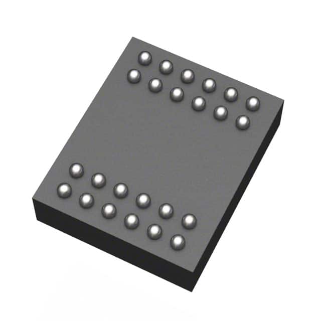
- Part No.:
- DS4000EC/WBGA
- Manufacturer:
- Analog Devices Inc./Maxim Integrated
- Category:
- Programmable Timers and Oscillators
- Package:
- 24-BBGA
- Datasheet:
-
 DS4000EC/WBGA.pdf
- Description:
- IC OSC TCXO 14.31818MHZ 24-BGA
- Quantity:
- Payment:

- Shipping:

Inventory:1,100
Please send an inquiry. Send us your inquiry, and we will respond immediately.
Product details
Overview
DS4000EC/WBGA from Maxim Integrated is a digitally controlled temperature-compensated crystal oscillator (DC-TCXO) with a fixed 14.31818 MHz F1 output, a programmable F2 output derived via integer division of F1, integrated 10-bit digital temperature sensor (±3°C accuracy), and 2-wire serial interface for frequency tuning and temperature readout. It operates from 0°C to +70°C and delivers ±1.0 ppm frequency stability over temperature.
For engineers reviewing the DS4000EC/WBGA datasheet, DS4000EC/WBGA pinout, DS4000EC/WBGA application, or DS4000EC/WBGA equivalent, key selection criteria include its dual-output TCXO architecture, ±10 ppm digital frequency tuning range, 24-pin WBGA package, CMOS square-wave outputs, and support for both standard (100 kHz) and fast-mode (400 kHz) I²C communication.
Technical Context
The DS4000EC/WBGA integrates a factory-calibrated TCXO core with on-die temperature sensing and digital compensation logic, enabling real-time frequency correction without external components. Its two independent outputs-F1 (fixed base frequency) and F2 (programmable via 5Dh register)-are both temperature-compensated and can be enabled/disabled independently using the TCXO Control Register (60h).
Frequency tuning is implemented via a signed 7-bit offset in the Frequency Tuning Register (66h), where each LSB corresponds to ~0.08 ppm, allowing ±10.16 ppm adjustment of the 14.31818 MHz base frequency. The 2-wire interface supports slave address configuration via A0 pin and operates at up to 400 kHz with open-drain SDA/SCL requiring external pullups.
Key Specifications
| Parameter | Value and Actual Design Meaning |
|---|---|
| Base Frequency (F1) | 14.31818 MHz - fixed, factory-trimmed output used as reference for F2 division |
| Frequency Stability | ±1.0 ppm from -40°C to +85°C - applies to both F1 and F2 outputs under industrial temp grade; DS4000EC/WBGA rated 0°C to +70°C |
| Digital Tuning Range | ±10.16 ppm - achieved via 7-bit signed offset in 66h register; enables microcontroller-based calibration |
| Temperature Sensing | 10-bit resolution (+0.25°C step), ±3°C accuracy - provides die temperature for compensation or system monitoring |
| I²C Interface Speed | Up to 400 kHz (Fast Mode) - supports high-speed register access; requires external pullup resistors on SDA/SCL |
| Output Type | CMOS square wave - F1 and F2 both deliver rail-to-rail digital outputs with 40–60% duty cycle |
| Supply Voltage | VCC = 4.75 V to 5.25 V - tight 5 V ±5% tolerance required for specified stability and current consumption |
Pinout & Package
DS4000EC/WBGA uses a 24-ball wafer-level BGA (WBGA) package with 1.27 mm pitch, solder-mask-defined pads (0.85 mm ball diameter), and 8.89 mm × 8.89 mm body size. Pin assignments follow JEDEC MO-220 standard per drawing 56-G6022-001A (V24-1 variation).
| Pin/Terminal | Circuit Role | Design Meaning |
|---|---|---|
| 1A, 1B, 1C, 1D, 2C, 2D | GND | Power ground for digital core; six dedicated pins reduce impedance and improve noise immunity |
| 2A, 2B | N.C. | No internal connection; must remain unconnected per datasheet - not tied to ground or voltage |
| 3A, 3B | GNDOSC | Separate ground for oscillator circuitry; isolation prevents digital switching noise from degrading phase noise |
| 3C, 3D | VOSC | Dedicated 5 V supply for oscillator section; decoupling required near these pins for stability |
| 4A, 4B | A0 | Hardware slave address bit; sets LSB of 7-bit I²C address (100010A0) to select between two device addresses |
| 4C, 4D | F1 | Fixed-frequency CMOS output (14.31818 MHz); always active unless disabled via TCXO Control Register (bit F1OE) |
| 5A, 5B | SDA | Open-drain bidirectional I²C data line; requires external pullup resistor (typically 4.7 kΩ) |
| 5C, 5D | VCC | Main 5 V supply for digital logic; separate from VOSC to enable independent power domain management |
| 6A, 6B | SCL | Open-drain I²C clock input; synchronized timing source for all register reads/writes |
| 6C, 6D | F2 | Programmable CMOS output; frequency set by FSR register (5Dh) as F1/(FSR+1) or F1/[2×(FSR+1)] |
Key Features
| Feature | Design Value |
|---|---|
| Dual temperature-compensated outputs | F1 (fixed) and F2 (programmable) both maintain ±1.0 ppm stability across operating temperature range |
| Integrated 10-bit temperature sensor | Provides on-die thermal data without external components; usable for system thermal management or self-calibration |
| Digital frequency tuning via I²C | ±10.16 ppm adjustment of base frequency using two's complement 7-bit offset register (66h) |
| Configurable F2 division ratio | Integer division of F1 by (FSR+1) or 2×(FSR+1) via DC bit in TCXO Control Register (60h) |
| Independent output enable control | F1OE and F2OE bits in register 60h allow dynamic power-down of either output to reduce system current |
Applications
| GPS Receivers | Wireless Base Stations |
|---|---|
Use Scenario: High-accuracy timing reference in handheld or vehicle-mounted GPS modules requiring stable 1PPS generation and low-jitter local oscillator. IC Role / Device Role / Timing Role: Primary TCXO providing 14.31818 MHz clock to GPS baseband processor and RF synthesizer; F2 used for UART or interface clocking. Use Value: ±1.0 ppm stability ensures minimal time error accumulation during cold starts and rapid satellite acquisition under varying ambient temperatures. | Use Scenario: Synchronization source in LTE/FDD or WCDMA small-cell base station radios where precise frequency alignment with network timing is mandatory. IC Role / Device Role / Timing Role: Dual-output TCXO supplying master clock (F1) to ADC/DAC and programmable clock (F2) to FPGA or PHY layer logic. Use Value: Digital tuning capability allows field calibration to compensate for aging drift and board-level thermal gradients, extending recalibration intervals. |
| Telecom Line Cards | SATCOM Terminals |
Use Scenario: Clock source for T1/E1 framers and jitter attenuators in carrier-grade access equipment deployed in temperature-variable central office environments. IC Role / Device Role / Timing Role: Fixed F1 output drives SERDES PLL; F2 provides configurable clock for packet processing engine or management MCU. Use Value: 24-pin WBGA footprint enables compact layout; integrated temperature sensor feeds host MCU for adaptive thermal derating algorithms. | Use Scenario: Reference oscillator in mobile SATCOM terminals mounted on aircraft or maritime vessels subject to wide thermal swings and vibration. IC Role / Device Role / Timing Role: Primary frequency reference for LNB downconverter LO synthesis and modem symbol clock generation. Use Value: Aging ≤1.0 ppm/year ensures long-term frequency holdover during signal loss; ±1.0 ppm/V supply stability maintains accuracy despite battery voltage sag. |
Equivalent & Alternatives
The following parts are listed as comparable options for similar digitally controlled TCXO applications.
| Alternative Part | Technical Difference | Application Difference | Selection Advice |
|---|---|---|---|
| DS4000GF/WBGA | Base frequency = 16.384 MHz; identical architecture, tuning range, and package | Targeted for telecom/datacom applications requiring 16.384 MHz (e.g., T1 framing, IEEE 1588 PTP clocks) | Select when system clock tree requires 16.384 MHz instead of 14.31818 MHz; no PCB or firmware changes needed beyond frequency register updates. |
| DS4000CW/WBGA | Base frequency = 12.800 MHz; same pinout, register map, and electrical specs | Optimized for wireless infrastructure and GPS where 12.8 MHz simplifies frequency planning for IF stages | Choose for cost-sensitive designs needing lower base frequency; retains full digital tuning and temperature sensing functionality. |
Compared with DS4000GF/WBGA and DS4000CW/WBGA, the DS4000EC/WBGA provides the exact 14.31818 MHz frequency required for NTSC video timing, legacy UART baud rate derivation (e.g., 115.2 kbps), and specific GPS chipset references - making it non-interchangeable without clock tree redesign.
Availability
DS4000EC/WBGA is available at Aetrix Electronics and suitable for GPS receivers, wireless base stations, telecom line cards, and SATCOM terminals requiring stable component supply with guaranteed long-term continuity.
Supply support for DS4000EC/WBGA includes scheduled delivery planning, volume procurement assistance, BOM continuity management, traceable sourcing, and lifecycle availability coordination for OEM customers, industrial embedded developers, connected-device designers, and electronics production programs.
Manufacturer
Maxim Integrated (now part of Analog Devices) designs precision analog and mixed-signal ICs for industrial, communications, and computing applications, with emphasis on high-reliability timing, power, and sensor solutions.
The DS4000EC/WBGA belongs to Maxim's digitally controlled TCXO product line, engineered specifically for systems demanding programmable, temperature-stable clock sources with integrated diagnostics and minimal external components.
FAQ
What is the base frequency of the DS4000EC/WBGA?
The DS4000EC/WBGA has a fixed base frequency of 14.31818 MHz on its F1 output. This value is laser-trimmed during manufacturing and marked on the device top as "DS4000EC". It serves as the reference for all F2 programmable outputs and digital tuning operations within the DS4000EC/WBGA.
Does the DS4000EC/WBGA require external components for temperature sensing?
No, the DS4000EC/WBGA includes a fully calibrated 10-bit digital temperature sensor with ±3°C accuracy and 0.25°C resolution. No external thermistors, ADCs, or calibration circuitry are needed - temperature data is read directly over the 2-wire interface using the READ TEMPERATURE command (address 64h) from the DS4000EC/WBGA.
Can both F1 and F2 outputs of the DS4000EC/WBGA operate simultaneously?
Yes, both F1 and F2 outputs of the DS4000EC/WBGA can operate simultaneously. Their enable states are independently controlled via bits F1OE and F2OE in the TCXO Control Register (60h). By default, both outputs are enabled at power-up, and either can be disabled dynamically via I²C to reduce system power consumption without affecting the other.
What is the maximum I²C clock speed supported by the DS4000EC/WBGA?
The DS4000EC/WBGA supports Fast Mode I²C operation up to 400 kHz, in addition to Standard Mode (100 kHz). Timing parameters such as tLOW, tHIGH, and tSU:DAT are fully specified for both modes in the datasheet. External pullup resistors must be sized appropriately - typically 4.7 kΩ - to meet rise/fall time requirements at 400 kHz for the DS4000EC/WBGA.
Is the DS4000EC/WBGA pin-compatible with other devices in the DS4000 family?
Yes, all DS4000 variants including DS4000EC/WBGA, DS4000GF/WBGA, and DS4000CW/WBGA share identical 24-ball WBGA packaging, pinout, register map, and electrical interface specifications. The only differences are base frequency and top-marking - making them hardware-compatible drop-in replacements when frequency requirements align, as confirmed in the Selector Guide for the DS4000EC/WBGA.
DS4000EC/WBGA Specifications
- Product attributes
- Attribute value
- Manufacturer:
- Analog Devices Inc./Maxim Integrated
- Series:
- -
- Package/Case:
- 24-BBGA
- Packaging:
- Bag
- Product Status:
- Obsolete
- Type:
- Temperature, Compensated Crystal Oscillator (TCXO)
- Count:
- -
- Frequency:
- 14.31818MHz
- Voltage - Supply:
- 4.75V ~ 5.25V
- Current - Supply:
- 1.5 mA
- Operating Temperature:
- 0°C ~ 70°C
- Supplier Device Package:
- 24-WBGA (11x9)
- Mounting Type:
- Surface Mount
- Grade:
- -
- Qualification:
- -
DS4000EC/WBGA FAQ
1.How can I place an order for DS4000EC/WBGA through Aetrix?
Please submit a Request for Quotation (RFQ) for DS4000EC/WBGA on Aetrix. Our sales agent will provide a competitive quotation and guide you through the order confirmation once you accept the terms.
2.Are the price and stock information for DS4000EC/WBGA reliable?
The price and inventory of DS4000EC/WBGA are updated periodically and may fluctuate due to market conditions. Stock and pricing data are typically refreshed every 24 hours. Quotation validity for DS4000EC/WBGA is usually 5 days.
3.What payment methods are accepted for DS4000EC/WBGA?
We accept Wire Transfer, PayPal, Credit Card, Western Union, MoneyGram, and Escrow for DS4000EC/WBGA transactions.
Note: Certain payment methods may incur a processing fee.
4.How is shipping managed for DS4000EC/WBGA?
DS4000EC/WBGA orders can be shipped via leading logistics carriers, including DHL, UPS, FedEx, TNT, or Registered Mail.
Once your DS4000EC/WBGA order is processed, you will receive an email with the shipment details and tracking number.
Note: Tracking information may take up to 24 hours to appear. Express delivery typically takes 3–5 business days.
5.How can I obtain technical support or documentation for DS4000EC/WBGA?
For technical support, including DS4000EC/WBGA datasheets, pinout diagrams, or application guidance, please contact our engineering support team. They can provide detailed documentation and assistance for your DS4000EC/WBGA requirements.
6.How does Aetrix verify that DS4000EC/WBGA is sourced from the original manufacturer or authorized distributors?
All DS4000EC/WBGA products on Aetrix are procured from qualified distributors and authorized channels. Our dedicated quality assurance team conducts strict verification, including traceability checks and, if necessary, third-party testing. This ensures that DS4000EC/WBGA meets industry standards.
7.What is the process for return or replacement of DS4000EC/WBGA?
All DS4000EC/WBGA units undergo pre-shipment inspection (PSI). If there is an issue with DS4000EC/WBGA, returns or replacements are accepted under the following conditions:
1.Quantity discrepancies, incorrect items, or visible external defects (such as breakage or corrosion), acknowledged by Aetrix.
2.The issue is reported within 90 days of delivery.
3.The DS4000EC/WBGA part is unused and in its original packaging.
Return procedure for DS4000EC/WBGA:
1.Submit a request within 90 days.
2.Obtain a Return Material Authorization (RMA) from Aetrix.
DS4000EC/WBGA Tags

-
NE555DR
Texas Instruments
-
SA555DR
Texas Instruments
-
NA555DR
Texas Instruments
-
SE555DR
Texas Instruments

-
NE555P
Texas Instruments

-
CD4541BM96
Texas Instruments

-
CD4541BE
Texas Instruments
-
TLC555QDR
Texas Instruments
-
TLC555IDR
Texas Instruments
-
TLC555QDRQ1
Texas Instruments

-
TPL5010DDCR
Texas Instruments
-
TLC555CP
Texas Instruments
Tech Hub

A practical engineering guide to 3.3V and 5V logic compatibility, input thresholds, resistor dividers, translator ICs, MOSFET level shifting, I2C pull-ups, timing limits and power-sequencing risks.

The 74HC595 uses push-pull logic outputs, while the TPIC6B595 uses 50 V open-drain DMOS sinks for higher-power loads. This guide compares timing, current limits, 3.3 V interfacing, load wiring, thermal…

The 74HC595 converts serial data into eight stable parallel outputs. This guide covers pin functions, shift and storage timing, OE and MR behavior, drive-current limits, cascading, voltage compatibilit…

A technical comparison of level-sensitive latches and edge-triggered flip-flops, covering timing windows, setup and hold limits, master–slave operation, time borrowing, race-through, HDL inference and…

A D latch stores one bit while Enable controls when data can pass. This reference covers gate-level operation, truth tables, transparency, setup and hold timing, LE versus OE, common ICs and practical …

An SR latch stores one bit through cross-coupled feedback. This engineering reference covers NOR and NAND implementations, truth tables, forbidden-state recovery, gated operation, switch debouncing, fa…

Latch circuits retain one bit through feedback. This technical reference covers SR and D latches, truth tables, transparency, timing limits, latch-versus-flip-flop behavior, applications and common log…

An engineering guide to LED driver operation, constant-current and constant-voltage outputs, linear and switching topologies, dimming, IC selection, calculations, replacement compatibility, and fault c…

Operational amplifier guide covering op amp basics, feedback, ideal vs real op amps, common configurations, buffer circuits, offset, bias current, gain-bandwidth, slew rate, rail-to-rail limits and sel…

Jumper cables guide covering safe connection order, red and black clamp placement, final ground connection, cable gauge, length, clamp quality, copper vs CCA cables, jump starter comparison and battery…


