
 My Inquiry
 My Account


Analog Devices Inc./Maxim Integrated DS4312P+
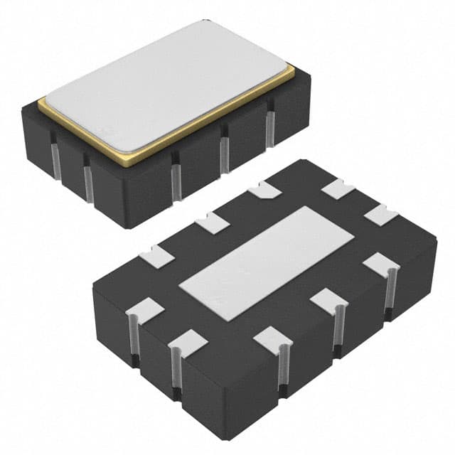
- Part No.:
- DS4312P+
- Manufacturer:
- Analog Devices Inc./Maxim Integrated
- Category:
- Programmable Timers and Oscillators
- Package:
- 10-LCCC Exposed Pad
- Datasheet:
-
 DS4312P+.pdf
- Description:
- IC OSC CLOCK 312.5MHZ 10LCCC
- Quantity:
- Payment:

- Shipping:

Inventory:1,193
Please send an inquiry. Send us your inquiry, and we will respond immediately.
Product details
Overview
DS4312P+ from Maxim Integrated is a 312.5MHz LVPECL-output ceramic surface-mount crystal oscillator with ±50ppm frequency stability, 3.3V operation, and <0.7psRMS phase jitter (12kHz–20MHz), designed for high-speed serial timing in SONET/SDH and 10GbE systems.
For engineers reviewing the DS4312P+ datasheet, DS4312P+ pinout, DS4312P+ application, or DS4312P+ equivalent, this page delivers verified package dimensions, LVPECL output drive specifications, startup time, thermal resistance, and RoHS-compliant LCCC pin mapping - all confirmed from Maxim's official DS4125–DS4776 datasheet Rev 2 (June 2008).
Technical Context
The DS4312P+ integrates an AT-cut fundamental-mode crystal with a BiPOLAR SiGe synthesizer IC to generate 312.5MHz output via PLL-based frequency synthesis. It supports active-high OE control with 200ns enable/disable propagation delay and operates across –40°C to +85°C.
Its LVPECL output stage drives 50Ω terminations at VCC – 2.0V bias, delivering 0.595–0.710V differential voltage, 45–55% duty cycle, and 200ps rise/fall times. Phase noise is –113dBc/Hz at 100kHz offset and –153dBc/Hz at 20MHz offset.
Key Specifications
| Parameter | Value and Actual Design Meaning |
|---|---|
| Output Frequency | 312.5MHz nominal - matches SONET OC-48/SDH STM-16 and 10GbE reference clock requirements. |
| Frequency Stability | ±50ppm total - covers temperature, aging, supply, and load variation over full industrial range. |
| Jitter (RMS) | <0.7ps (12kHz–20MHz) - ensures low BER in high-speed serial links like InfiniBand and GPON. |
| Supply Voltage | 3.3V ±5% - compatible with standard logic rails; ICC = 74–100mA depending on load condition. |
| Operating Temp | –40°C to +85°C - qualified for telecom infrastructure and industrial embedded timing applications. |
| Package | 5.0mm × 3.2mm × 1.49mm, 10-pin LCCC - compact ceramic SMT footprint with exposed paddle (non-connected). |
| Output Type | LVPECL - differential signaling with PECL_BIAS = VCC – 2.0V; requires external 50Ω termination to bias point. |
Pinout & Package
DS4312P+ uses a 10-pin LCCC ceramic package (5.0mm × 3.2mm × 1.49mm) with non-connected exposed paddle (EP). Pin 1 is OE (active-high enable); pins 4 and 5 are complementary LVPECL outputs (OUTP/OUTN); pin 6 is VCC; pin 3 is GND; pins 2 and 7–10 are no-connect (must be floated).
| Pin/Terminal | Circuit Role | Design Meaning |
|---|---|---|
| 1 | OE | Active-high output enable with internal 100kΩ pullup - drives outputs to PECL_BIAS level when low. |
| 2, 7–10 | N.C. | No connection - must remain unconnected and unbonded per Maxim design guidance. |
| 3 | GND | Ground reference for power and signal integrity - connects directly to substrate ground plane. |
| 4 | OUTP | Positive LVPECL output - requires 50Ω termination to PECL_BIAS (VCC – 2.0V) for valid logic levels. |
| 5 | OUTN | Negative LVPECL output - complements OUTP; differential pair defines timing edge precision. |
| 6 | VCC | 3.3V supply input - bypass with 0.01μF and 0.1μF capacitors close to pin per typical operating circuit. |
| EP | Exposed Paddle | Thermal pad not electrically connected - must not be soldered or placed over metal layers. |
Key Features
| Feature | Design Value |
|---|---|
| Ultra-low phase jitter | <0.7psRMS (12kHz–20MHz) - minimizes timing uncertainty in 10GbE and SONET clock recovery. |
| LVPECL output interface | Valid logic swing with 50Ω termination to VCC – 2.0V - enables direct interfacing with TI, IDT, and Broadcom SerDes inputs. |
| Industrial temperature range | –40°C to +85°C operation - supports deployment in carrier-grade optical line cards and base station timing modules. |
| RoHS-compliant packaging | Lead-free JESD97 e4 finish (Au over Ni) - compatible with leaded and lead-free reflow profiles per IPC/JEDEC J-STD-020. |
| Fundamental-mode crystal + PLL | AT-cut quartz resonator with integrated SiGe synthesizer - eliminates external loop filter components and reduces BOM count. |
Applications
| InfiniBand Timing Module | GPON Optical Line Terminal (OLT) |
|---|---|
Use Scenario: Provides reference clock for InfiniBand switch fabric PHY layer with sub-1ps jitter tolerance. IC Role / Device Role / Timing Role: Primary system clock source for 10Gbps serial lanes with deterministic phase alignment. Use Value: 312.5MHz output and <0.7psRMS jitter meet InfiniBand DDR specification for interconnect latency and BER performance. | Use Scenario: Synchronizes upstream burst transmission in GPON OLTs requiring precise 312.5MHz frame timing. IC Role / Device Role / Timing Role: Master timing reference for TDMA slot allocation and burst-mode receiver calibration. Use Value: ±50ppm stability over temperature ensures consistent upstream frame alignment across –40°C to +85°C cabinet environments. |
| 10GbE LAN/WAN PHY | SONET OC-48/SDH STM-16 Equipment |
Use Scenario: Supplies clock to 10GBASE-R PCS/PMA layer in enterprise routers and data center switches. IC Role / Device Role / Timing Role: Low-jitter reference oscillator for 64b/66b encoding and SERDES CDR lock acquisition. Use Value: LVPECL output drive strength and 200ps edge rates support clean signal integrity on FR4 backplanes up to 24″. | Use Scenario: Generates line-rate clock for SONET OC-48 add/drop multiplexers and SDH STM-16 regenerators. IC Role / Device Role / Timing Role: Stratum-3-equivalent timing source with holdover capability during network synchronization loss. Use Value: –113dBc/Hz phase noise at 100kHz offset suppresses adjacent-channel interference in dense wavelength division multiplexing (DWDM) systems. |
Equivalent & Alternatives
The following parts are listed as comparable options for similar crystal oscillator applications.
| Alternative Part | Technical Difference | Application Difference | Selection Advice |
|---|---|---|---|
| IDT XLP726A312M5000 | 312.5MHz LVPECL XO, ±25ppm stability, 0.5psRMS jitter (12kHz–20MHz), 3.3V, 5.0×3.2mm 6-pin SMD | Higher stability and lower jitter, but 6-pin package lacks OE control and N.C. flexibility of DS4312P+ | Select when tighter frequency accuracy and lowest possible jitter are prioritized over enable functionality. |
| SiTime SiT8208AI-23-33E-312.500000Y | 312.5MHz LVPECL MEMS oscillator, ±50ppm stability, 0.8psRMS jitter, 3.3V, 5.0×3.2mm 6-pin SMD | MEMS-based architecture offers superior shock/vibration immunity but slightly higher jitter than DS4312P+ | Select for harsh-environment deployments where mechanical robustness outweighs marginal jitter trade-off. |
Compared with IDT XLP726A312M5000 and SiTime SiT8208AI-23-33E-312.500000Y, DS4312P+ provides unique OE control and 10-pin LCCC layout for legacy board compatibility, while maintaining industry-standard jitter and stability for telecom timing - making it optimal for drop-in upgrades in existing DS4-XO designs.
Availability
DS4312P+ is available at Aetrix Electronics and suitable for SONET/SDH line cards, 10GbE switches, GPON OLTs, and InfiniBand fabric modules requiring stable component supply, long-term lifecycle assurance, and RoHS-compliant timing solutions.
Supply support for DS4312P+ includes scheduled delivery planning, volume procurement assistance, BOM continuity management, traceable sourcing, and lifecycle availability coordination for OEM customers, industrial embedded developers, connected-device designers, and electronics production programs.
Manufacturer
Maxim Integrated (now part of Analog Devices) is a U.S.-based semiconductor company specializing in analog, mixed-signal, and timing solutions for industrial, communications, and computing markets.
The DS4-XO series - including DS4312P+ - was engineered specifically for high-reliability telecom and datacom timing applications demanding ultra-low jitter, wide temperature operation, and LVDS/LVPECL interoperability.
FAQ
What output type does DS4312P+ use, and how is it terminated?
DS4312P+ uses LVPECL output, requiring 50Ω termination from each output (OUTP and OUTN) to the PECL_BIAS voltage level at VCC – 2.0V. This configuration ensures valid differential logic levels and maintains signal integrity for high-speed interfaces. The DS4312P+ datasheet specifies 0.595–0.710V differential swing under these conditions, and the device's internal design assumes this bias point for proper operation.
What is the frequency stability specification for DS4312P+, and what factors does it include?
The DS4312P+ has a total frequency stability of ±50ppm, covering combined effects of temperature variation (±35ppm), initial tolerance (±20ppm), supply voltage change (±3ppm/V), load variation (±1ppm), and 15-year aging (±7ppm). This value is explicitly defined in the DS4125–DS4776 datasheet's Electrical Characteristics table and applies across the full –40°C to +85°C operating range with 3.3V ±5% supply.
Does DS4312P+ have an output enable function, and how does it behave?
Yes, DS4312P+ features an active-high Output Enable (OE) pin with internal 100kΩ pullup. When OE is low, LVPECL outputs go to the PECL_BIAS level (VCC – 2.0V); when high, outputs become active with specified differential swing. Propagation delays are tPZA = 200ns (enable) and tPAZ = 200ns (disable), both guaranteed by design per the DS4312P+ datasheet.
What is the package type and thermal resistance of DS4312P+?
DS4312P+ uses a 10-pin LCCC ceramic package measuring 5.0mm × 3.2mm × 1.49mm with a non-connected exposed paddle (EP). Its junction-to-ambient thermal resistance (θJA) is 90°C/W, as documented in the "Chip Information" section of the DS4125–DS4776 datasheet. This value guides thermal design for continuous operation within rated ambient limits.
Is DS4312P+ RoHS-compliant, and what is its lead finish?
Yes, DS4312P+ is RoHS-compliant with a lead-free JESD97 category e4 finish (gold over nickel). This finish is compatible with both lead-based and lead-free soldering processes, and the + suffix in DS4312P+ explicitly denotes compliance per Maxim's ordering nomenclature and datasheet revision history.
DS4312P+ Specifications
- Product attributes
- Attribute value
- Manufacturer:
- Analog Devices Inc./Maxim Integrated
- Series:
- DS4-XO
- Package/Case:
- 10-LCCC Exposed Pad
- Packaging:
- Tray
- Product Status:
- Obsolete
- Type:
- Clock Oscillator
- Count:
- -
- Frequency:
- 312.5MHz
- Voltage - Supply:
- 3.135V ~ 3.465V
- Current - Supply:
- 49 mA
- Operating Temperature:
- -40°C ~ 85°C
- Supplier Device Package:
- 10-LCCC (5x3.2)
- Mounting Type:
- Surface Mount
- Grade:
- -
- Qualification:
- -
DS4312P+ FAQ
1.How can I place an order for DS4312P+ through Aetrix?
Please submit a Request for Quotation (RFQ) for DS4312P+ on Aetrix. Our sales agent will provide a competitive quotation and guide you through the order confirmation once you accept the terms.
2.Are the price and stock information for DS4312P+ reliable?
The price and inventory of DS4312P+ are updated periodically and may fluctuate due to market conditions. Stock and pricing data are typically refreshed every 24 hours. Quotation validity for DS4312P+ is usually 5 days.
3.What payment methods are accepted for DS4312P+?
We accept Wire Transfer, PayPal, Credit Card, Western Union, MoneyGram, and Escrow for DS4312P+ transactions.
Note: Certain payment methods may incur a processing fee.
4.How is shipping managed for DS4312P+?
DS4312P+ orders can be shipped via leading logistics carriers, including DHL, UPS, FedEx, TNT, or Registered Mail.
Once your DS4312P+ order is processed, you will receive an email with the shipment details and tracking number.
Note: Tracking information may take up to 24 hours to appear. Express delivery typically takes 3–5 business days.
5.How can I obtain technical support or documentation for DS4312P+?
For technical support, including DS4312P+ datasheets, pinout diagrams, or application guidance, please contact our engineering support team. They can provide detailed documentation and assistance for your DS4312P+ requirements.
6.How does Aetrix verify that DS4312P+ is sourced from the original manufacturer or authorized distributors?
All DS4312P+ products on Aetrix are procured from qualified distributors and authorized channels. Our dedicated quality assurance team conducts strict verification, including traceability checks and, if necessary, third-party testing. This ensures that DS4312P+ meets industry standards.
7.What is the process for return or replacement of DS4312P+?
All DS4312P+ units undergo pre-shipment inspection (PSI). If there is an issue with DS4312P+, returns or replacements are accepted under the following conditions:
1.Quantity discrepancies, incorrect items, or visible external defects (such as breakage or corrosion), acknowledged by Aetrix.
2.The issue is reported within 90 days of delivery.
3.The DS4312P+ part is unused and in its original packaging.
Return procedure for DS4312P+:
1.Submit a request within 90 days.
2.Obtain a Return Material Authorization (RMA) from Aetrix.
DS4312P+ Tags

-
NE555DR
Texas Instruments
-
SA555DR
Texas Instruments
-
NA555DR
Texas Instruments
-
SE555DR
Texas Instruments

-
NE555P
Texas Instruments

-
CD4541BM96
Texas Instruments

-
CD4541BE
Texas Instruments
-
TLC555QDR
Texas Instruments
-
TLC555IDR
Texas Instruments
-
TLC555QDRQ1
Texas Instruments

-
TPL5010DDCR
Texas Instruments
-
TLC555CP
Texas Instruments
Tech Hub

A practical engineering guide to 3.3V and 5V logic compatibility, input thresholds, resistor dividers, translator ICs, MOSFET level shifting, I2C pull-ups, timing limits and power-sequencing risks.

The 74HC595 uses push-pull logic outputs, while the TPIC6B595 uses 50 V open-drain DMOS sinks for higher-power loads. This guide compares timing, current limits, 3.3 V interfacing, load wiring, thermal…

The 74HC595 converts serial data into eight stable parallel outputs. This guide covers pin functions, shift and storage timing, OE and MR behavior, drive-current limits, cascading, voltage compatibilit…

A technical comparison of level-sensitive latches and edge-triggered flip-flops, covering timing windows, setup and hold limits, master–slave operation, time borrowing, race-through, HDL inference and…

A D latch stores one bit while Enable controls when data can pass. This reference covers gate-level operation, truth tables, transparency, setup and hold timing, LE versus OE, common ICs and practical …

An SR latch stores one bit through cross-coupled feedback. This engineering reference covers NOR and NAND implementations, truth tables, forbidden-state recovery, gated operation, switch debouncing, fa…

Latch circuits retain one bit through feedback. This technical reference covers SR and D latches, truth tables, transparency, timing limits, latch-versus-flip-flop behavior, applications and common log…

An engineering guide to LED driver operation, constant-current and constant-voltage outputs, linear and switching topologies, dimming, IC selection, calculations, replacement compatibility, and fault c…

Operational amplifier guide covering op amp basics, feedback, ideal vs real op amps, common configurations, buffer circuits, offset, bias current, gain-bandwidth, slew rate, rail-to-rail limits and sel…

Jumper cables guide covering safe connection order, red and black clamp placement, final ground connection, cable gauge, length, clamp quality, copper vs CCA cables, jump starter comparison and battery…


