
 My Inquiry
 My Account


Analog Devices Inc./Maxim Integrated DS5002FMN-16+
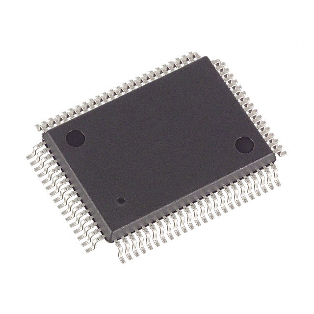
- Part No.:
- DS5002FMN-16+
- Manufacturer:
- Analog Devices Inc./Maxim Integrated
- Category:
- Microcontrollers
- Package:
- 80-BQFP
- Datasheet:
-
 DS5002FMN-16+.pdf
- Description:
- IC MCU 8BIT EXTRNL NVSRAM 80QFP
- Quantity:
- Payment:

- Shipping:

Inventory:1,243
Please send an inquiry. Send us your inquiry, and we will respond immediately.
Product details
Overview
DS5002FMN-16+ from Maxim Integrated (now Analog Devices) is an 8051-compatible secure microprocessor with 128kB nonvolatile SRAM, on-chip 64-bit encryption engine, self-destruct input (SDI), and lithium-backed power-fail protection. It operates from -40°C to +85°C, supports in-system programming via on-chip serial port, and maintains memory integrity for >10 years without external power. Used in tamper-resistant embedded systems requiring firmware confidentiality and crash-proof operation.
For engineers reviewing the DS5002FMN-16+ datasheet, DS5002FMN-16+ pinout, DS5002FMN-16+ application, or DS5002FMN-16+ equivalent, key selection considerations include industrial temperature range (-40°C to +85°C), Pb-free 80-pin QFP package, battery-backed nonvolatile RAM retention, SDI-triggered key erasure, and compatibility with DS5001FP-based designs requiring enhanced security.
Technical Context
The DS5002FMN-16+ implements real-time address and data encryption/decryption using a protected 64-bit key loaded from an on-chip true random-number generator - no user-accessible key exposure. Its architecture extends the DS5001FP soft microprocessor with mandatory security enforcement: all program/data accesses to external byte-wide NV SRAM are encrypted, and Vector RAM + encryption keys are erased upon SDI activation or tamper detection.
It features dual power domains: VCC-powered operation and VLI (lithium cell)-backed retention mode. When VCC drops below VLI, VCCO switches to VLI to sustain SRAM and internal registers; PF and VRST signals assert to coordinate system-level power-down sequencing. The device supports expanded bus timing at up to 16MHz and includes early-warning power-fail interrupt, watchdog timer, and crash-proof reset behavior.
Key Specifications
| Parameter | Value and Actual Design Meaning |
|---|---|
| Oscillator Frequency | Up to 16MHz - enables full-speed 8051 execution with zero-cycle encryption overhead. |
| Nonvolatile SRAM Capacity | 128kB - configured as program and/or data storage; retained >10 years via lithium backup (VLI = 2.5–4.0V). |
| Operating Temperature | -40°C to +85°C - qualified for industrial environments; matches DS5002FMN-16+ ordering code. |
| Encryption Key | 64-bit, internally generated - never exposed externally; erased on SDI assertion or physical attack attempt. |
| Self-Destruct Input (SDI) | Active-high deglitched input - triggers immediate erasure of Vector RAM and encryption key, even with VCC = 0V. |
| Power-Fail Warning | VPFW = 4.1–4.6V - provides early interrupt before VCC falls below VCCMIN (3.85–4.25V), enabling graceful shutdown. |
| Package | 80-pin QFP - RoHS-compliant, Pb-free; pinout identical to DS5002FPM-16+ but rated for extended temperature. |
Pinout & Package
DS5002FMN-16+ uses an 80-pin Quad Flat Package (QFP) with 0.65mm pitch, thermally enhanced for industrial operation. Pin functions are fully defined per Maxim DS5002FP datasheet Rev 072806.
| Pin/Terminal | Circuit Role | Design Meaning |
|---|---|---|
| P0.0–P0.7 | Multiplexed Address/Data Bus (AD0–AD7) | Open-drain I/O; serves as lower byte of address/data bus in expanded mode; requires external pullups when used as GPIO. |
| BA0–BA14 | Byte-Wide Address Bus (A0–A14) | Nonmultiplexed 15-bit address lines; directly connect to 8k/32k/128k SRAM; CE2/CE3 repurposed as A15/A16 for 128k config. |
| BD0–BD7 | Byte-Wide Data Bus (D0–D7) | Bidirectional 8-bit data path to SRAM or peripherals; supports MOVX instructions and RPC read/write cycles. |
| R/W, RD, WR | Memory Control Strobes | Active-low R/W controls SRAM write enable; RD/WR strobes synchronize expanded bus read/write timing per AC specs. |
| SDI | Self-Destruct Trigger | Active-high input with 4–50µs deglitch window; asserts irreversible key/Vector RAM erase regardless of VCC state. |
| VLI, VCCO | Lithium Backup Interface | VLI accepts 2.5–4.0V lithium cell; VCCO auto-switches between VCC and VLI to sustain SRAM during power loss. |
| VRST, PF | Power-Fail Status Outputs | VRST = logic 0 indicates VCC < VCCMIN; PF = logic 0 confirms switch to lithium backup - both guaranteed at VCC = 0V. |
Key Features
| Feature | Design Value |
|---|---|
| On-chip 64-bit true random key generator | Eliminates key injection risk; key never exits chip - required for FIPS-140-2 Level 3-aligned tamper resistance. |
| Real-time encryption/decryption engine | Zero-cycle penalty vs. DS5001FP - logical addresses and data bytes encrypted/decrypted transparently during fetch/execute/write. |
| Lithium-backed nonvolatile SRAM | 128kB retained >10 years at room temp using single 3V Li cell; VCCO switching ensures uninterrupted power to SRAM. |
| Crash-proof power management | Power-fail reset, early-warning interrupt, and watchdog timer prevent corruption during brownout or abrupt power loss. |
| Optional die top coating (DS5002FPM variant) | Physically blocks microprobe access to silicon; DS5002FMN-16+ supports same security architecture but omits coating. |
Applications
| Secure Firmware Storage | Industrial Telematics Module |
|---|---|
Use Scenario: Storing proprietary bootloader and application firmware in field-deployed edge devices subject to physical inspection. IC Role / Device Role / Timing Role: Secure microprocessor executing encrypted code from battery-backed SRAM; manages boot sequence and runtime decryption. Use Value: Prevents firmware reverse-engineering via bus snooping or memory dump; SDI integration enables hardware-triggered wipe on enclosure breach. |
Use Scenario: Remote monitoring unit in oil/gas pipeline SCADA systems operating across -40°C to +85°C ambient. IC Role / Device Role / Timing Role: Primary controller with crash-proof data logging - retains sensor history and configuration during grid outages. Use Value: >10-year SRAM retention eliminates need for EEPROM wear leveling; PF/VRST signals coordinate backup power switchover without software intervention. |
| Payment Terminal Security Core | Medical Device Secure Boot |
Use Scenario: EMV-compliant payment terminal requiring PCI PTS v6.0 tamper-evident design and key lifecycle control. IC Role / Device Role / Timing Role: Root-of-trust processor validating signed firmware images and managing cryptographic keys in isolated memory. Use Value: On-chip 64-bit DES-derived encryption and automatic key erasure on SDI meet PCI PTS physical security requirements for key storage. |
Use Scenario: FDA Class II infusion pump storing calibration data and safety-critical control algorithms in nonvolatile memory. IC Role / Device Role / Timing Role: Safety-certified microcontroller ensuring deterministic boot and runtime integrity via encrypted program space. Use Value: Crash-proof operation prevents data loss during power interruption; encrypted Vector RAM blocks unauthorized vector table modification. |
Equivalent & Alternatives
The following parts are listed as comparable options for similar secure microprocessor applications.
| Alternative Part | Technical Difference | Application Difference | Selection Advice |
|---|---|---|---|
| DS5002FPM-16+ | Same core, identical pinout and firmware, but rated 0°C to +70°C and includes optional die top coating for microprobe resistance. | Preferred for commercial-grade secure modules where extended temperature is not required and maximum physical tamper resistance is critical. | Select DS5002FPM-16+ only if operating environment stays within 0°C–70°C and top-coating is mandated by security policy. |
| MAX32550 | ARM Cortex-M3-based secure MCU with Trust Protection Unit (TPU), AES-256, and secure boot - no lithium-backed SRAM or SDI pin. | Targets modern secure IoT endpoints needing high-performance crypto acceleration and OS support, not legacy 8051 firmware porting. | Choose MAX32550 for new designs requiring TLS stack, secure firmware updates, and ARM ecosystem tooling - not as drop-in replacement. |
Compared with DS5002FPM-16+, DS5002FMN-16+ trades top-coating and commercial temp range for industrial qualification and broader environmental deployment. Against MAX32550, it offers deterministic 8051 compatibility and lithium-backed persistence but lacks modern crypto accelerators and secure boot infrastructure.
Availability
DS5002FMN-16+ is available at Aetrix Electronics and suitable for industrial control systems, secure payment terminals, medical data loggers, and military communications equipment requiring stable component supply across extended temperature ranges and long product lifecycles.
Supply support for DS5002FMN-16+ includes scheduled delivery planning, volume procurement assistance, BOM continuity management, traceable sourcing, and lifecycle availability coordination for OEM customers, industrial embedded developers, connected-device designers, and electronics production programs.
Manufacturer
Maxim Integrated, now part of Analog Devices, designs precision analog, mixed-signal, and secure ICs for industrial, automotive, and communications markets.
The DS5002FP family was developed to provide tamper-resistant, lithium-backed microprocessor solutions for applications demanding firmware confidentiality, crash-proof data retention, and physical attack resilience - especially where legacy 8051 codebases must be secured without architectural overhaul.
FAQ
What is the operating temperature range of the DS5002FMN-16+?
The DS5002FMN-16+ is specified for industrial operation from -40°C to +85°C, as confirmed in the Ordering Information table and Absolute Maximum Ratings section of the Maxim DS5002FP datasheet Rev 072806. This distinguishes it from the commercial-grade DS5002FPM-16+, which operates from 0°C to +70°C. The DS5002FMN-16+ maintains full functionality - including encryption, SRAM retention, and SDI response - across this full range.
Does the DS5002FMN-16+ include lithium backup capability?
Yes, the DS5002FMN-16+ integrates lithium backup functionality via dedicated VLI (lithium voltage input) and VCCO (VCC output) pins. When VCC drops below VLI, the internal switch automatically routes power from the lithium cell to VCCO, sustaining the 128kB NV SRAM and internal registers. Data retention exceeds 10 years at room temperature, and the PF and VRST outputs signal backup activation - all guaranteed even at VCC = 0V.
How does the self-destruct input (SDI) function on the DS5002FMN-16+?
The SDI pin on the DS5002FMN-16+ is an active-high, deglitched input that triggers irreversible erasure of the 64-bit encryption key and 48-byte Vector RAM upon assertion - regardless of VCC presence. Per AC Characteristics, pulses must exceed tSPA (min 10µs at VCC > 4.5V, 50µs at VCC = 0V) to guarantee activation. The DS5002FMN-16+ implements hardware-level tamper response: no firmware involvement is required, and the action occurs even during power-off states.
Is the DS5002FMN-16+ pin-compatible with the DS5001FP?
Yes, the DS5002FMN-16+ is pin-compatible and instruction-set compatible with the DS5001FP 128k soft microprocessor, as explicitly stated in the General Description and Block Diagram sections. All I/O, bus, and control pins match identically, allowing direct PCB replacement. However, DS5002FMN-16+ adds security-specific pins (SDI, VRST, PF) and modifies behavior of CE2/CE3 for 128k SRAM addressing - requiring firmware validation for full feature utilization.
What package type and lead finish does the DS5002FMN-16+ use?
The DS5002FMN-16+ uses an 80-pin Quad Flat Package (QFP) with 0.65mm lead pitch and Pb-free (RoHS-compliant) finish, as indicated by the "+" suffix in the part number per Maxim's ordering guide. The package is identical in footprint and thermal characteristics to DS5002FPM-16+, enabling shared PCB layouts across temperature grades. No lead finish exceptions or special handling requirements are specified beyond standard JEDEC J-STD-020 reflow profiles.
DS5002FMN-16+ Specifications
- Product attributes
- Attribute value
- Manufacturer:
- Analog Devices Inc./Maxim Integrated
- Package/Case:
- 80-BQFP
- Series:
- DS500x
- Packaging:
- Tray
- Product Status:
- Obsolete
- Programmable:
- Not Verified
- Core Processor:
- 8051
- Core Size:
- 8-Bit
- Speed:
- 16MHz
- Connectivity:
- EBI/EMI, SIO, UART/USART
- Peripherals:
- Power-Fail Reset, WDT
- Number of I/O:
- 32
- Program Memory Size:
- External
- Program Memory Type:
- NVSRAM
- EEPROM Size:
- -
- RAM Size:
- -
- Voltage - Supply (Vcc/Vdd):
- 4.5V ~ 5.5V
- Data Converters:
- -
- Oscillator Type:
- External
- Operating Temperature:
- -40°C ~ 85°C (TA)
- Grade:
- -
- Qualification:
- -
- Mounting Type:
- Surface Mount
- Supplier Device Package:
DS5002FMN-16+ FAQ
1.How can I place an order for DS5002FMN-16+ through Aetrix?
Please submit a Request for Quotation (RFQ) for DS5002FMN-16+ on Aetrix. Our sales agent will provide a competitive quotation and guide you through the order confirmation once you accept the terms.
2.Are the price and stock information for DS5002FMN-16+ reliable?
The price and inventory of DS5002FMN-16+ are updated periodically and may fluctuate due to market conditions. Stock and pricing data are typically refreshed every 24 hours. Quotation validity for DS5002FMN-16+ is usually 5 days.
3.What payment methods are accepted for DS5002FMN-16+?
We accept Wire Transfer, PayPal, Credit Card, Western Union, MoneyGram, and Escrow for DS5002FMN-16+ transactions.
Note: Certain payment methods may incur a processing fee.
4.How is shipping managed for DS5002FMN-16+?
DS5002FMN-16+ orders can be shipped via leading logistics carriers, including DHL, UPS, FedEx, TNT, or Registered Mail.
Once your DS5002FMN-16+ order is processed, you will receive an email with the shipment details and tracking number.
Note: Tracking information may take up to 24 hours to appear. Express delivery typically takes 3–5 business days.
5.How can I obtain technical support or documentation for DS5002FMN-16+?
For technical support, including DS5002FMN-16+ datasheets, pinout diagrams, or application guidance, please contact our engineering support team. They can provide detailed documentation and assistance for your DS5002FMN-16+ requirements.
6.How does Aetrix verify that DS5002FMN-16+ is sourced from the original manufacturer or authorized distributors?
All DS5002FMN-16+ products on Aetrix are procured from qualified distributors and authorized channels. Our dedicated quality assurance team conducts strict verification, including traceability checks and, if necessary, third-party testing. This ensures that DS5002FMN-16+ meets industry standards.
7.What is the process for return or replacement of DS5002FMN-16+?
All DS5002FMN-16+ units undergo pre-shipment inspection (PSI). If there is an issue with DS5002FMN-16+, returns or replacements are accepted under the following conditions:
1.Quantity discrepancies, incorrect items, or visible external defects (such as breakage or corrosion), acknowledged by Aetrix.
2.The issue is reported within 90 days of delivery.
3.The DS5002FMN-16+ part is unused and in its original packaging.
Return procedure for DS5002FMN-16+:
1.Submit a request within 90 days.
2.Obtain a Return Material Authorization (RMA) from Aetrix.
DS5002FMN-16+ Tags

-
ATTINY4-TSHR
Microchip Technology
-
ATTINY10-TSHR
Microchip Technology
-
ATTINY10-TS8R
Microchip Technology

-
ATTINY202-SSNR
Microchip Technology
-
ATTINY202-SSFR
Microchip Technology
-
ATTINY402-SSNR
Microchip Technology

-
PIC16F15213T-I/MF
Microchip Technology
-
PIC16F15213-E/MF
Microchip Technology

-
PIC10F200T-I/OT
Microchip Technology
-
ATTINY412-SSNR
Microchip Technology
-
PIC10F202T-I/OT
Microchip Technology

-
ATTINY404-SSNR
Microchip Technology
Tech Hub

A practical engineering guide to 3.3V and 5V logic compatibility, input thresholds, resistor dividers, translator ICs, MOSFET level shifting, I2C pull-ups, timing limits and power-sequencing risks.

The 74HC595 uses push-pull logic outputs, while the TPIC6B595 uses 50 V open-drain DMOS sinks for higher-power loads. This guide compares timing, current limits, 3.3 V interfacing, load wiring, thermal…

The 74HC595 converts serial data into eight stable parallel outputs. This guide covers pin functions, shift and storage timing, OE and MR behavior, drive-current limits, cascading, voltage compatibilit…

A technical comparison of level-sensitive latches and edge-triggered flip-flops, covering timing windows, setup and hold limits, master–slave operation, time borrowing, race-through, HDL inference and…

A D latch stores one bit while Enable controls when data can pass. This reference covers gate-level operation, truth tables, transparency, setup and hold timing, LE versus OE, common ICs and practical …

An SR latch stores one bit through cross-coupled feedback. This engineering reference covers NOR and NAND implementations, truth tables, forbidden-state recovery, gated operation, switch debouncing, fa…

Latch circuits retain one bit through feedback. This technical reference covers SR and D latches, truth tables, transparency, timing limits, latch-versus-flip-flop behavior, applications and common log…

An engineering guide to LED driver operation, constant-current and constant-voltage outputs, linear and switching topologies, dimming, IC selection, calculations, replacement compatibility, and fault c…

Operational amplifier guide covering op amp basics, feedback, ideal vs real op amps, common configurations, buffer circuits, offset, bias current, gain-bandwidth, slew rate, rail-to-rail limits and sel…

Jumper cables guide covering safe connection order, red and black clamp placement, final ground connection, cable gauge, length, clamp quality, copper vs CCA cables, jump starter comparison and battery…


