
 My Inquiry
 My Account


Analog Devices Inc./Maxim Integrated DS5002FPM-16
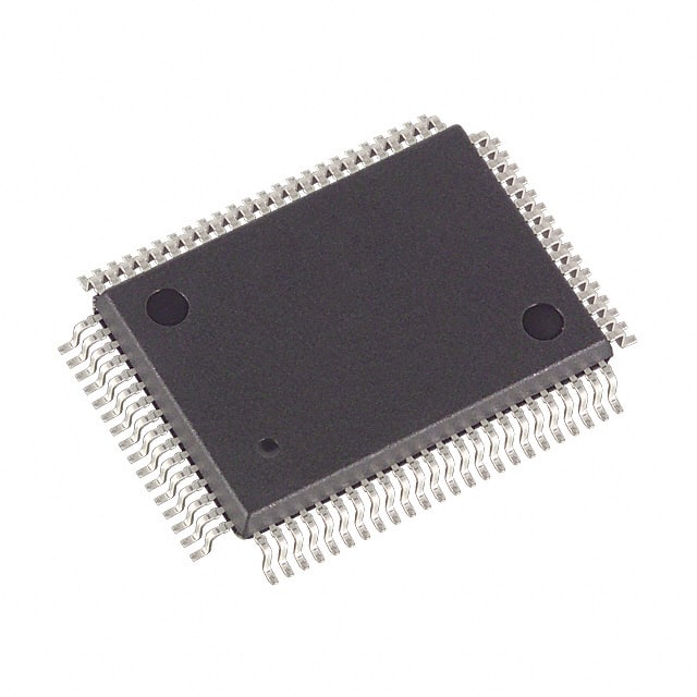
- Part No.:
- DS5002FPM-16
- Manufacturer:
- Analog Devices Inc./Maxim Integrated
- Category:
- Microcontrollers
- Package:
- 80-BQFP
- Datasheet:
-
 DS5002FPM-16.pdf
- Description:
- IC MCU 8BIT EXTRNL NVSRAM 80QFP
- Quantity:
- Payment:

- Shipping:

Inventory:3,808
Please send an inquiry. Send us your inquiry, and we will respond immediately.
Product details
Overview
DS5002FPM-16 from Maxim Integrated (now Analog Devices) is an 8051-compatible secure microprocessor with 128kB nonvolatile SRAM, on-chip 64-bit encryption engine, self-destruct input (SDI), and lithium-backed power-fail protection. It operates at up to 16MHz, supports in-system programming via serial port, and maintains memory integrity for >10 years without external power - deployed in tamper-resistant financial terminals and secure authentication modules.
For engineers reviewing the DS5002FPM-16 datasheet, DS5002FPM-16 pinout, DS5002FPM-16 application, or DS5002FPM-16 equivalent, key selection considerations include lithium-backed NV SRAM retention, SDI-triggered key erasure, encrypted bus operation, 80 QFP package compatibility, and crash-proof reset behavior under brownout conditions.
Technical Context
The DS5002FPM-16 implements real-time address and data encryption using a protected 64-bit key loaded by an on-chip true random-number generator. Its byte-wide bus (BA14–BA0 + BD7–BD0) accesses external SRAM while presenting scrambled physical addresses and encrypted data values - all transparent to software execution.
Security enforcement includes hardware-level SDI deglitching (tSPA ≥ 50µs at VCC = 0V), lithium-backed CE1/CE2/CE3/PE1/PE2 enabling persistent chip-select during power loss, and automatic key erasure upon SDI activation or security lock reset - ensuring no residual key exposure after tamper event.
Key Specifications
| Parameter | Value and Actual Design Meaning |
|---|---|
| Oscillator Frequency | Up to 16MHz - enables full-speed 8051 instruction execution with zero overhead from real-time encryption/decryption. |
| NV SRAM Capacity | 128kB - configured via MSEL pin; accessed as encrypted program/data space with lithium-backed retention >10 years. |
| Encryption Key | 64-bit on-chip key - generated by true random-number generator; never exposed externally; erased on SDI assertion or lock reset. |
| Power-Fail Detection | VCCMIN = 4.09V (industrial), VPFW = 4.12V - triggers early-warning interrupt and VRST/ PF outputs before brownout resets CPU. |
| SDI Pulse Accept | tSPA ≥ 50µs at VCC = 0V - ensures reliable self-destruct activation even during complete power loss with lithium backup active. |
| Operating Voltage | VCC = 4.5V to 5.5V - compatible with standard 5V logic systems; VLI input accepts 2.5V–4.0V lithium cell for backup. |
| Package | 80-pin QFP - surface-mount footprint with defined thermal and mechanical characteristics per JEDEC MS-026. |
Pinout & Package
DS5002FPM-16 uses an 80-pin Quad Flat Package (QFP) with 0.65mm lead pitch, compliant with JEDEC MS-026. The package provides full access to 8-bit bidirectional data bus (BD7–BD0), 15-bit nonmultiplexed address bus (BA14–BA0), four lithium-backed chip enables (CE1–CE4), two lithium-backed peripheral enables (PE1–PE2), and dedicated security pins including SDI and VRST.
| Pin/Terminal | Circuit Role | Design Meaning |
|---|---|---|
| P0.0–P0.7 | Multiplexed Address/Data Bus / I/O Port 0 | Open-drain port requiring external pullups; serves as AD0–AD7 during multiplexed bus cycles; drives BA0–BA7 when demultiplexed. |
| BA14–BA0 | Nonmultiplexed Address Bus | Direct connection to SRAM address inputs; BA13/BA14 unused with 8k RAM; CE2/CE3 repurposed as A16/A15 for 128k configuration. |
| BD7–BD0 | Byte-Wide Data Bus | Bidirectional 8-bit path to SRAM; carries encrypted data during read/write; isolated from VCCO during lithium-backup mode. |
| CE1–CE4, PE1–PE2 | Lithium-Backed Chip/Peripheral Enables | Remain logic-high during VCC loss to prevent spurious writes; CE1/CE2/CE3/PE1/PE2 retain state via VLI; PE3/PE4 require external hold circuitry. |
| SDI | Self-Destruct Input | Active-high input with deglitching; assertion erases Vector RAM and 64-bit key regardless of VCC presence; must be grounded if unused. |
| VRST, PF | Power-Fail Status Outputs | VRST goes low when VCC < VCCMIN - guarantees reset signal even at VCC = 0V; PF indicates switch to lithium backup mode. |
Key Features
| Feature | Design Value |
|---|---|
| Real-time bus encryption | Logical-to-physical address translation and per-byte data encryption performed in hardware with zero CPU cycle penalty. |
| True random key generation | On-chip entropy source loads 64-bit key prior to firmware loading - key value never exposed to user or debug interface. |
| Lithium-backed nonvolatile retention | SRAM contents preserved >10 years at room temperature using single 3V lithium cell; VLI input range 2.5V–4.0V. |
| Crash-proof reset architecture | Power-fail interrupt, watchdog timer, and early-warning reset ensure deterministic state recovery during brownout or abrupt power loss. |
| Top-coating option (DS5002FPM) | Die-level epoxy coating prevents microprobe access to internal metal layers - physically blocks reverse-engineering attempts. |
Applications
| Financial Transaction Terminal | Secure Identity Authentication Module |
|---|---|
|
Use Scenario: Embedded controller in PIN pad or smart card reader handling cryptographic keys and transaction signing. IC Role / Device Role / Timing Role: Secure execution environment for ISO/IEC 7816-4 applets; performs AES/RSA operations on encrypted SRAM-resident keys. Use Value: Prevents extraction of private keys via bus monitoring or physical probing; SDI integration with tamper mesh ensures immediate key erasure on enclosure breach. |
Use Scenario: Trusted platform module (TPM) companion in government ID issuance systems storing biometric templates and digital certificates. IC Role / Device Role / Timing Role: Tamper-resistant storage and runtime execution host for FIPS 140-2 Level 3 validated firmware. Use Value: Lithium-backed 128kB NV SRAM retains certificate chains across power cycles; encrypted bus prevents side-channel leakage during template loading. |
| Industrial Control Security Coprocessor | Medical Device Firmware Vault |
|
Use Scenario: Standalone security enforcer in PLC or RTU validating firmware signatures before boot and protecting configuration parameters. IC Role / Device Role / Timing Role: Secure bootloader and runtime key manager interfacing with main MCU via serial port or parallel bus. Use Value: In-system reprogramming capability allows field updates without exposing decrypted firmware; MSEL-configurable memory map supports legacy 32k or modern 128k SRAM. |
Use Scenario: Embedded vault in diagnostic imaging equipment safeguarding calibration coefficients and regulatory compliance logs. IC Role / Device Role / Timing Role: Nonvolatile storage controller with write-protection enforced by R/W pin and memory partitioning. Use Value: Crash-proof operation ensures log integrity during unexpected shutdown; VRST output synchronizes safe shutdown sequence with main system controller. |
Equivalent & Alternatives
The following parts are listed as comparable options for similar secure microprocessor applications.
| Alternative Part | Technical Difference | Application Difference | Selection Advice |
|---|---|---|---|
| DS5002FMN-16 | Wider industrial temperature range (-40°C to +85°C); identical pinout, encryption, and memory architecture. | Suitable for outdoor kiosks or automotive-adjacent infrastructure where ambient temperature exceeds 70°C. | Select DS5002FMN-16 when operating outside 0°C–70°C commercial range; otherwise DS5002FPM-16 offers cost-optimized qualification. |
| MAX32550 | ARM Cortex-M3 core, 512kB flash, hardware crypto accelerators (AES-256, SHA-256), but no lithium-backed SRAM or SDI pin. | Targets higher-performance secure boot and TLS stack execution; lacks DS5002FPM-16's physical tamper response and 10-year battery-backed retention. | Choose MAX32550 for modern cryptographic protocol support; DS5002FPM-16 remains preferred where physical tamper resistance and ultra-long-term NV retention are mandatory. |
Compared with DS5002FMN-16, DS5002FPM-16 trades extended temperature rating for lower cost and commercial qualification; compared with MAX32550, it sacrifices ARM ecosystem compatibility and advanced crypto algorithms for deterministic physical security, SDI-driven key destruction, and guaranteed 10-year lithium-backed data retention without software intervention.
Availability
DS5002FPM-16 is available at Aetrix Electronics and suitable for financial terminal manufacturing, secure identity credentialing, and industrial control system development requiring stable component supply and long-term lifecycle assurance.
Supply support for DS5002FPM-16 includes scheduled delivery planning, volume procurement assistance, BOM continuity management, traceable sourcing, and lifecycle availability coordination for OEM customers, industrial embedded developers, connected-device designers, and electronics production programs.
Manufacturer
Maxim Integrated (acquired by Analog Devices in 2021) designs high-reliability analog and mixed-signal ICs for security, power, and sensing applications.
The DS5002FPM-16 belongs to Maxim's secure microprocessor family, engineered specifically for applications demanding physical tamper resistance, cryptographic key protection, and battery-backed nonvolatile memory retention without external supervision.
FAQ
What is the primary security mechanism used by the DS5002FPM-16 to protect stored firmware?
The DS5002FPM-16 protects firmware using real-time hardware encryption of both address and data buses. All program and data stored in its 128kB external SRAM is encrypted using a 64-bit key generated by an on-chip true random-number generator. Logical addresses are translated to scrambled physical addresses, and each data byte is encrypted based on its location and key - making bus snooping ineffective. This encryption is active during both loading and execution, and the key is erased immediately upon SDI activation or security lock reset.
Does the DS5002FPM-16 require an external crystal, or can it use an external clock source?
The DS5002FPM-16 supports both configurations: it can drive a quartz crystal between XTAL1 and XTAL2 (1.0–16MHz), or accept an external CMOS clock signal applied to XTAL1 with XTAL2 left unconnected. AC timing specifications confirm valid operation with external clock high/low times ≥15ns at 16MHz, and rise/fall times ≤15ns - enabling direct connection to precision clock generators or FPGA outputs without additional buffering.
How does the DS5002FPM-16 maintain memory integrity during power loss?
The DS5002FPM-16 maintains memory integrity during power loss via lithium-backed circuitry tied to the VLI pin. When VCC drops below VLI (typically 3.0V), internal switches route power from the lithium cell to VCCO, CE1–CE4, PE1–PE2, and VRST/PF outputs. This preserves SRAM contents, chip-enable states, and reset signaling for over 10 years at room temperature. The PF pin asserts low to isolate non-battery-backed peripherals, while VRST guarantees a clean reset signal even at VCC = 0V.
What is the function of the MSEL pin on the DS5002FPM-16, and how does it affect memory configuration?
The MSEL pin on the DS5002FPM-16 selects between two memory architectures: when pulled to VCC (5V), the device expects four 32kB SRAM chips addressed via CE1–CE4; when grounded, it configures for a single 128kB SRAM where CE2 and CE3 become address lines A16 and A15. This pin must be hardwired - floating or incorrect bias causes undefined memory mapping and boot failure. The DS5002FPM-16 datasheet specifies that MSEL state is sampled at power-up and latched for the duration of operation.
Can the DS5002FPM-16 be programmed in-circuit, and what interface is used?
Yes, the DS5002FPM-16 supports in-system programming via its on-chip UART interface (P3.0/RXD and P3.1/TXD). Programming is initiated by asserting the PROG pin low at power-up or issuing the "Z" command to clear the security lock, then using the "L" command to load encrypted firmware through the serial port. The bootstrap loader handles encryption transparently - no external encryptor is needed. The process requires only 5V power, ground, and the two UART signals; no JTAG or SWD interface is present.
DS5002FPM-16 Specifications
- Product attributes
- Attribute value
- Manufacturer:
- Analog Devices Inc./Maxim Integrated
- Package/Case:
- 80-BQFP
- Series:
- DS500x
- Packaging:
- Tray
- Product Status:
- Obsolete
- Programmable:
- Not Verified
- Core Processor:
- 8051
- Core Size:
- 8-Bit
- Speed:
- 16MHz
- Connectivity:
- EBI/EMI, SIO, UART/USART
- Peripherals:
- Power-Fail Reset, WDT
- Number of I/O:
- 32
- Program Memory Size:
- External
- Program Memory Type:
- NVSRAM
- EEPROM Size:
- -
- RAM Size:
- 128K x 8
- Voltage - Supply (Vcc/Vdd):
- 4.5V ~ 5.5V
- Data Converters:
- -
- Oscillator Type:
- External
- Operating Temperature:
- 0°C ~ 70°C (TA)
- Grade:
- -
- Qualification:
- -
- Mounting Type:
- Surface Mount
- Supplier Device Package:
DS5002FPM-16 FAQ
1.How can I place an order for DS5002FPM-16 through Aetrix?
Please submit a Request for Quotation (RFQ) for DS5002FPM-16 on Aetrix. Our sales agent will provide a competitive quotation and guide you through the order confirmation once you accept the terms.
2.Are the price and stock information for DS5002FPM-16 reliable?
The price and inventory of DS5002FPM-16 are updated periodically and may fluctuate due to market conditions. Stock and pricing data are typically refreshed every 24 hours. Quotation validity for DS5002FPM-16 is usually 5 days.
3.What payment methods are accepted for DS5002FPM-16?
We accept Wire Transfer, PayPal, Credit Card, Western Union, MoneyGram, and Escrow for DS5002FPM-16 transactions.
Note: Certain payment methods may incur a processing fee.
4.How is shipping managed for DS5002FPM-16?
DS5002FPM-16 orders can be shipped via leading logistics carriers, including DHL, UPS, FedEx, TNT, or Registered Mail.
Once your DS5002FPM-16 order is processed, you will receive an email with the shipment details and tracking number.
Note: Tracking information may take up to 24 hours to appear. Express delivery typically takes 3–5 business days.
5.How can I obtain technical support or documentation for DS5002FPM-16?
For technical support, including DS5002FPM-16 datasheets, pinout diagrams, or application guidance, please contact our engineering support team. They can provide detailed documentation and assistance for your DS5002FPM-16 requirements.
6.How does Aetrix verify that DS5002FPM-16 is sourced from the original manufacturer or authorized distributors?
All DS5002FPM-16 products on Aetrix are procured from qualified distributors and authorized channels. Our dedicated quality assurance team conducts strict verification, including traceability checks and, if necessary, third-party testing. This ensures that DS5002FPM-16 meets industry standards.
7.What is the process for return or replacement of DS5002FPM-16?
All DS5002FPM-16 units undergo pre-shipment inspection (PSI). If there is an issue with DS5002FPM-16, returns or replacements are accepted under the following conditions:
1.Quantity discrepancies, incorrect items, or visible external defects (such as breakage or corrosion), acknowledged by Aetrix.
2.The issue is reported within 90 days of delivery.
3.The DS5002FPM-16 part is unused and in its original packaging.
Return procedure for DS5002FPM-16:
1.Submit a request within 90 days.
2.Obtain a Return Material Authorization (RMA) from Aetrix.
DS5002FPM-16 Tags

-
ATTINY4-TSHR
Microchip Technology
-
ATTINY10-TSHR
Microchip Technology
-
ATTINY10-TS8R
Microchip Technology

-
ATTINY202-SSNR
Microchip Technology
-
ATTINY202-SSFR
Microchip Technology
-
ATTINY402-SSNR
Microchip Technology

-
PIC16F15213T-I/MF
Microchip Technology
-
PIC16F15213-E/MF
Microchip Technology

-
PIC10F200T-I/OT
Microchip Technology
-
ATTINY412-SSNR
Microchip Technology
-
PIC10F202T-I/OT
Microchip Technology

-
ATTINY404-SSNR
Microchip Technology
Tech Hub

A practical engineering guide to 3.3V and 5V logic compatibility, input thresholds, resistor dividers, translator ICs, MOSFET level shifting, I2C pull-ups, timing limits and power-sequencing risks.

The 74HC595 uses push-pull logic outputs, while the TPIC6B595 uses 50 V open-drain DMOS sinks for higher-power loads. This guide compares timing, current limits, 3.3 V interfacing, load wiring, thermal…

The 74HC595 converts serial data into eight stable parallel outputs. This guide covers pin functions, shift and storage timing, OE and MR behavior, drive-current limits, cascading, voltage compatibilit…

A technical comparison of level-sensitive latches and edge-triggered flip-flops, covering timing windows, setup and hold limits, master–slave operation, time borrowing, race-through, HDL inference and…

A D latch stores one bit while Enable controls when data can pass. This reference covers gate-level operation, truth tables, transparency, setup and hold timing, LE versus OE, common ICs and practical …

An SR latch stores one bit through cross-coupled feedback. This engineering reference covers NOR and NAND implementations, truth tables, forbidden-state recovery, gated operation, switch debouncing, fa…

Latch circuits retain one bit through feedback. This technical reference covers SR and D latches, truth tables, transparency, timing limits, latch-versus-flip-flop behavior, applications and common log…

An engineering guide to LED driver operation, constant-current and constant-voltage outputs, linear and switching topologies, dimming, IC selection, calculations, replacement compatibility, and fault c…

Operational amplifier guide covering op amp basics, feedback, ideal vs real op amps, common configurations, buffer circuits, offset, bias current, gain-bandwidth, slew rate, rail-to-rail limits and sel…

Jumper cables guide covering safe connection order, red and black clamp placement, final ground connection, cable gauge, length, clamp quality, copper vs CCA cables, jump starter comparison and battery…


