
 My Inquiry
 My Account


Analog Devices Inc./Maxim Integrated DS5003-CS1+
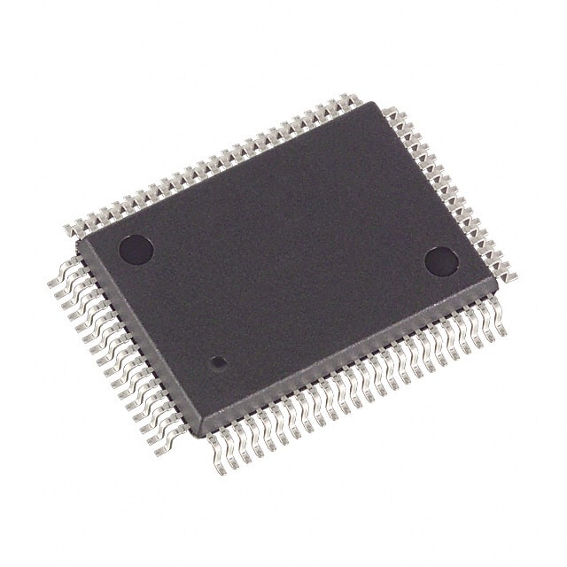
- Part No.:
- DS5003-CS1+
- Manufacturer:
- Analog Devices Inc./Maxim Integrated
- Category:
- Microcontrollers
- Package:
- 80-BQFP
- Datasheet:
-
 DS5003-CS1+.pdf
- Description:
- IC MCU 8BIT EXTRNL NVSRAM 80QFP
- Quantity:
- Payment:

- Shipping:

Inventory:1,788
Please send an inquiry. Send us your inquiry, and we will respond immediately.
Product details
Overview
DS5003-CS1+ from Maxim Integrated is an 8051-compatible secure microprocessor with lithium-backed nonvolatile SRAM, 256 bytes of on-chip RAM (128 direct + 128 indirect), 64-bit on-chip encryption key, self-destruct input (SDI), and crash-proof operation preserving data >10 years without power. It executes encrypted code from external SRAM in gaming machines and software-protection-critical systems.
For engineers reviewing the DS5003-CS1+ datasheet, DS5003-CS1+ pinout, DS5003-CS1+ application, or DS5003-CS1+ equivalent, this page delivers verified technical context, real-time encryption architecture details, lithium-backed bus timing, SDI pulse acceptance thresholds, and validated alternatives for secure embedded firmware deployment.
Technical Context
The DS5003-CS1+ implements real-time hardware encryption/decryption of all byte-wide address and data bus transactions using a protected 64-bit key generated by an on-chip true random-number generator. Its memory map supports up to 128kB external SRAM (64kB program + 64kB data), accessed via nonmultiplexed BA0–BA14 and BD0–BD7 buses with CE1–CE4 and PE1–PE4 chip/peripheral enables.
Security enforcement includes automatic erasure of vector SRAM and encryption key upon SDI activation (tSPA ≥ 10 μs at VCC = 0V), top-die coating to prevent microprobing, and power-fail detection with early-warning interrupt (VPFW = 4.25–4.50 V) and reset (VCCMIN = 4.00–4.25 V). The device operates from 1.0–16.0 MHz and maintains full functionality during lithium backup (VLI = 2.5–4.0 V).
Key Specifications
| Parameter | Value and Actual Design Meaning |
|---|---|
| Oscillator Frequency | 1.0–16.0 MHz - Enables flexible clocking for performance vs. power trade-offs in battery-backed systems. |
| Nonvolatile SRAM Capacity | Up to 128kB - Configurable as 64kB program + 64kB data storage, converted to lithium-backed NV memory. |
| On-Chip RAM | 256 bytes total (128 direct + 128 indirect) - Supports stack operations and register-indirect addressing (R0/R1) for 8051-compliant firmware. |
| Encryption Key | 64-bit on-chip key - Generated by true random-number generator; erased on tamper attempt, ensuring no persistent key exposure. |
| SDI Pulse Accept Threshold | tSPA ≥ 10 μs at VCC = 0V - Guarantees reliable self-destruct activation even during complete power loss. |
| Power-Fail Warning Voltage | VPFW = 4.25–4.50 V - Triggers early-warning interrupt before VCC drops below operational minimum (4.00–4.25 V). |
| Lithium Backup Voltage | VLI = 2.5–4.0 V - Powers critical security logic and retains SRAM contents for >10 years at room temperature. |
Pinout & Package
DS5003-CS1+ is housed in an 80-pin MQFP (Metric Quad Flat Package) with 0.65 mm lead pitch, RoHS-compliant and lead-free per + suffix. Pin functions are fully defined per Maxim's official pin description table (Rev 0, March 2008).
| Pin/Terminal | Circuit Role | Design Meaning |
|---|---|---|
| VCC / VCCO / VLI / GND | Power domain management | VCCO switches between VCC and VLI to maintain SRAM power; VLI supplies lithium cell voltage (2.5–4.0 V); GND is logic reference. |
| P0.0–P0.7 / P1.0–P1.7 / P2.0–P2.7 / P3.0–P3.7 | General-purpose I/O with dual functions | P0 serves as multiplexed AD0–AD7 or open-drain address/data bus; P2 provides A8–A15; P3 includes UART (RXD/TXD), INT0/INT1, T0/T1, WR/RD. |
| BA0–BA14 / BD0–BD7 / CE1–CE4 / PE1–PE4 | Byte-wide memory/peripheral interface | Nonmultiplexed 15-bit address (BA0–BA14) and 8-bit data (BD0–BD7) bus; CE1–CE4 enable up to four 32kB SRAM blocks; PE1–PE4 access peripheral memory regions under PES control. |
| SDI / VRST / PF / PROG / RST / ALE / R/W | Security and control signaling | SDI triggers irreversible key/SRAM erasure; VRST signals low-VCC reset state; PF indicates lithium backup active; PROG invokes bootstrap loader; RST is active-high reset; ALE latches P0 address; R/W controls SRAM write enable. |
| XTAL1 / XTAL2 | Crystal oscillator interface | Connects to external crystal (1–16 MHz); XTAL1 is inverter input, XTAL2 is output - defines system clock source independent of VCC stability. |
Key Features
| Feature | Design Value |
|---|---|
| Real-time bus encryption | All BA/BD bus traffic encrypted/decrypted on-the-fly using address- and key-dependent algorithm - prevents observation of logical program flow or data patterns. |
| Lithium-backed nonvolatile retention | Preserves SRAM contents and security state for >10 years at 25°C with 3V lithium cell - eliminates need for external EEPROM or flash in secure boot applications. |
| Self-destruct on tamper | SDI activation (≥10 μs high pulse) erases 64-bit key and 48-byte vector SRAM regardless of VCC presence - ensures zero residual secret exposure. |
| Crash-proof power management | Power-fail reset + early-warning interrupt + watchdog timer guarantee deterministic recovery from brownout or sudden power loss - critical for unattended systems. |
| Bootstrap loader with security lock | In-system programming via serial port; U command clears lock to erase key/SRAM; L command loads scrambled firmware - enforces secure update workflow. |
Applications
| Gaming Machine Security Module | Pay-TV Conditional Access Unit |
|---|---|
Use Scenario: Tamper-resistant execution of game logic and payout algorithms in slot machines and video lottery terminals. IC Role / Device Role / Timing Role: Secure microprocessor executing encrypted firmware from lithium-backed SRAM; manages cryptographic keys and responds to physical intrusion sensors via SDI. Use Value: Prevents firmware extraction and unauthorized modification through on-chip encryption, self-destruct, and die coating - meets GLI-11 and IGT security mandates. |
Use Scenario: Decryption of encrypted broadcast streams and enforcement of subscription entitlements in set-top boxes. IC Role / Device Role / Timing Role: Root-of-trust controller storing and applying conditional access keys; interfaces with secure peripherals via PE1–PE4 under PES control. Use Value: Ensures keys remain inaccessible during probing or voltage glitching attacks, with guaranteed erasure on SDI assertion - satisfies DVB-CI and ETSI TS 101 693 requirements. |
| Industrial Firmware Protection System | Medical Device Bootloader Controller |
Use Scenario: Secure boot and runtime integrity verification for programmable logic controllers and HMIs in factory automation. IC Role / Device Role / Timing Role: Primary secure MCU managing encrypted application load from external SRAM; uses R/W, CE1–CE4, and BA/BD bus for deterministic memory access. Use Value: Eliminates risk of malicious firmware injection by enforcing encrypted execution and crash-proof retention - supports IEC 62443-3-3 SL2 compliance. |
Use Scenario: Certified bootloader for Class II/III medical devices requiring secure firmware updates and audit-trail logging. IC Role / Device Role / Timing Role: Trusted execution environment with power-fail reset and >10-year data retention; stores cryptographic signatures and update metadata in protected SRAM. Use Value: Maintains regulatory traceability and prevents rollback attacks via immutable key erasure on tamper - aligns with FDA Cybersecurity Guidance and IEC 62304 SW Level C. |
Equivalent & Alternatives
The following parts are listed as comparable options for similar secure microprocessor applications.
| Alternative Part | Technical Difference | Application Difference | Selection Advice |
|---|---|---|---|
| DS5002FP+ | 128 bytes total RAM (no indirect scratchpad); identical encryption, SDI, lithium backup, and bus interface. | Lacks 128-byte indirect RAM - unsuitable for stack-heavy 8051 firmware requiring >128B local storage. | Select DS5002FP+ only when application firmware fits within 128B direct RAM and avoids register-indirect addressing beyond 0x7F. |
| MAX3667EVKIT+ | Evaluation kit for MAX3667 secure microcontroller; not a direct IC replacement - contains DS5003-compatible support circuitry and debug interface. | Used for prototyping and validation, not production deployment; requires separate DS5003-CS1+ for final design. | Use MAX3667EVKIT+ to verify secure boot flow and SDI response before committing to DS5003-CS1+ layout; not a functional substitute. |
Compared with DS5002FP+, DS5003-CS1+ adds essential indirect RAM for robust 8051 stack handling without increasing package size or power; compared with MAX3667EVKIT+, it is the production-grade silicon enabling certified, field-deployable security - not a development tool.
Availability
DS5003-CS1+ is available at Aetrix Electronics and suitable for gaming machine security modules, pay-TV conditional access units, industrial firmware protection systems, and medical device bootloader controllers requiring stable component supply and long-term lifecycle assurance.
Supply support for DS5003-CS1+ includes scheduled delivery planning, volume procurement assistance, BOM continuity management, traceable sourcing, and lifecycle availability coordination for OEM customers, industrial embedded developers, connected-device designers, and electronics production programs.
Manufacturer
Maxim Integrated (now part of Analog Devices) designs precision analog, mixed-signal, and secure semiconductor solutions for industrial, communications, and computing applications.
The DS5003-CS1+ belongs to Maxim's secure microprocessor product line, engineered specifically for applications demanding cryptographic firmware protection, tamper-evident operation, and decade-long nonvolatile data retention without external backup power sources.
FAQ
What is the function of the SDI pin on the DS5003-CS1+?
The SDI (Self-Destruct Input) pin on the DS5003-CS1+ triggers irreversible erasure of the 64-bit encryption key and 48-byte vector SRAM when asserted high for ≥10 μs - even with VCC = 0V. This ensures zero residual secret exposure during physical tampering. DS5003-CS1+ guarantees this behavior across its full operating range and is designed to interface directly with external tamper-detection circuits.
How does the DS5003-CS1+ achieve crash-proof operation?
The DS5003-CS1+ achieves crash-proof operation through three integrated mechanisms: (1) power-fail reset that activates below VCCMIN (4.00–4.25 V), (2) early-warning power-fail interrupt triggered at VPFW (4.25–4.50 V), and (3) watchdog timer with configurable timeout. These features ensure deterministic recovery and data integrity during brownouts or sudden power loss - a core requirement for DS5003-CS1+ deployments in unattended systems.
Can the DS5003-CS1+ execute code directly from external SRAM?
Yes, the DS5003-CS1+ executes encrypted code directly from external SRAM via its byte-wide BA0–BA14/BD0–BD7 bus. All address and data transactions are encrypted/decrypted in real time using the on-chip 64-bit key, making the logical program flow unintelligible to external observers. This capability is fundamental to DS5003-CS1+'s role in secure boot and runtime protection architectures.
What is the purpose of the VRST pin on the DS5003-CS1+?
The VRST pin on the DS5003-CS1+ is an open-drain I/O that drives low when VCC falls below VCCMIN (4.00–4.25 V), indicating an active reset state due to undervoltage. Because DS5003-CS1+ retains functionality during lithium backup, VRST remains valid even at VCC = 0V - enabling synchronized power-down resets across multiple DS5003-CS1+ devices in a system.
Does the DS5003-CS1+ support in-system programming?
Yes, the DS5003-CS1+ supports in-system programming through its on-chip serial port (P3.0/RXD and P3.1/TXD) using the bootstrap loader invoked by a falling edge on the PROG pin. Firmware is loaded in scrambled (encrypted) form and requires the security lock to be cleared first - a process that erases the existing key and vector SRAM. This workflow is integral to DS5003-CS1+'s secure update model.
DS5003-CS1+ Specifications
- Product attributes
- Attribute value
- Manufacturer:
- Analog Devices Inc./Maxim Integrated
- Package/Case:
- 80-BQFP
- Series:
- DS500x
- Packaging:
- Tray
- Product Status:
- Obsolete
- Programmable:
- Not Verified
- Core Processor:
- 8051
- Core Size:
- 8-Bit
- Speed:
- 16MHz
- Connectivity:
- EBI/EMI, SIO, UART/USART
- Peripherals:
- Power-Fail Reset, WDT
- Number of I/O:
- 32
- Program Memory Size:
- External
- Program Memory Type:
- NVSRAM
- EEPROM Size:
- -
- RAM Size:
- -
- Voltage - Supply (Vcc/Vdd):
- 4V ~ 5.5V
- Data Converters:
- -
- Oscillator Type:
- External
- Operating Temperature:
- 0°C ~ 70°C (TA)
- Grade:
- -
- Qualification:
- -
- Mounting Type:
- Surface Mount
- Supplier Device Package:
DS5003-CS1+ FAQ
1.How can I place an order for DS5003-CS1+ through Aetrix?
Please submit a Request for Quotation (RFQ) for DS5003-CS1+ on Aetrix. Our sales agent will provide a competitive quotation and guide you through the order confirmation once you accept the terms.
2.Are the price and stock information for DS5003-CS1+ reliable?
The price and inventory of DS5003-CS1+ are updated periodically and may fluctuate due to market conditions. Stock and pricing data are typically refreshed every 24 hours. Quotation validity for DS5003-CS1+ is usually 5 days.
3.What payment methods are accepted for DS5003-CS1+?
We accept Wire Transfer, PayPal, Credit Card, Western Union, MoneyGram, and Escrow for DS5003-CS1+ transactions.
Note: Certain payment methods may incur a processing fee.
4.How is shipping managed for DS5003-CS1+?
DS5003-CS1+ orders can be shipped via leading logistics carriers, including DHL, UPS, FedEx, TNT, or Registered Mail.
Once your DS5003-CS1+ order is processed, you will receive an email with the shipment details and tracking number.
Note: Tracking information may take up to 24 hours to appear. Express delivery typically takes 3–5 business days.
5.How can I obtain technical support or documentation for DS5003-CS1+?
For technical support, including DS5003-CS1+ datasheets, pinout diagrams, or application guidance, please contact our engineering support team. They can provide detailed documentation and assistance for your DS5003-CS1+ requirements.
6.How does Aetrix verify that DS5003-CS1+ is sourced from the original manufacturer or authorized distributors?
All DS5003-CS1+ products on Aetrix are procured from qualified distributors and authorized channels. Our dedicated quality assurance team conducts strict verification, including traceability checks and, if necessary, third-party testing. This ensures that DS5003-CS1+ meets industry standards.
7.What is the process for return or replacement of DS5003-CS1+?
All DS5003-CS1+ units undergo pre-shipment inspection (PSI). If there is an issue with DS5003-CS1+, returns or replacements are accepted under the following conditions:
1.Quantity discrepancies, incorrect items, or visible external defects (such as breakage or corrosion), acknowledged by Aetrix.
2.The issue is reported within 90 days of delivery.
3.The DS5003-CS1+ part is unused and in its original packaging.
Return procedure for DS5003-CS1+:
1.Submit a request within 90 days.
2.Obtain a Return Material Authorization (RMA) from Aetrix.
DS5003-CS1+ Tags

-
ATTINY4-TSHR
Microchip Technology
-
ATTINY10-TSHR
Microchip Technology
-
ATTINY10-TS8R
Microchip Technology

-
ATTINY202-SSNR
Microchip Technology
-
ATTINY202-SSFR
Microchip Technology
-
ATTINY402-SSNR
Microchip Technology

-
PIC16F15213T-I/MF
Microchip Technology
-
PIC16F15213-E/MF
Microchip Technology

-
PIC10F200T-I/OT
Microchip Technology
-
ATTINY412-SSNR
Microchip Technology
-
PIC10F202T-I/OT
Microchip Technology

-
ATTINY404-SSNR
Microchip Technology
Tech Hub

A practical engineering guide to 3.3V and 5V logic compatibility, input thresholds, resistor dividers, translator ICs, MOSFET level shifting, I2C pull-ups, timing limits and power-sequencing risks.

The 74HC595 uses push-pull logic outputs, while the TPIC6B595 uses 50 V open-drain DMOS sinks for higher-power loads. This guide compares timing, current limits, 3.3 V interfacing, load wiring, thermal…

The 74HC595 converts serial data into eight stable parallel outputs. This guide covers pin functions, shift and storage timing, OE and MR behavior, drive-current limits, cascading, voltage compatibilit…

A technical comparison of level-sensitive latches and edge-triggered flip-flops, covering timing windows, setup and hold limits, master–slave operation, time borrowing, race-through, HDL inference and…

A D latch stores one bit while Enable controls when data can pass. This reference covers gate-level operation, truth tables, transparency, setup and hold timing, LE versus OE, common ICs and practical …

An SR latch stores one bit through cross-coupled feedback. This engineering reference covers NOR and NAND implementations, truth tables, forbidden-state recovery, gated operation, switch debouncing, fa…

Latch circuits retain one bit through feedback. This technical reference covers SR and D latches, truth tables, transparency, timing limits, latch-versus-flip-flop behavior, applications and common log…

An engineering guide to LED driver operation, constant-current and constant-voltage outputs, linear and switching topologies, dimming, IC selection, calculations, replacement compatibility, and fault c…

Operational amplifier guide covering op amp basics, feedback, ideal vs real op amps, common configurations, buffer circuits, offset, bias current, gain-bandwidth, slew rate, rail-to-rail limits and sel…

Jumper cables guide covering safe connection order, red and black clamp placement, final ground connection, cable gauge, length, clamp quality, copper vs CCA cables, jump starter comparison and battery…


