
 My Inquiry
 My Account


Analog Devices Inc./Maxim Integrated DS8500-JND+
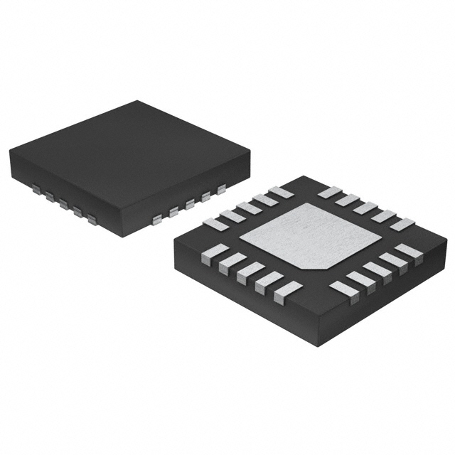
- Part No.:
- DS8500-JND+
- Manufacturer:
- Analog Devices Inc./Maxim Integrated
- Category:
- Specialized
- Package:
- 20-WQFN Exposed Pad
- Datasheet:
-
 DS8500-JND+.pdf
- Description:
- IC INTERFACE SPECIALIZED 20TQFN
- Quantity:
- Payment:

- Shipping:

Inventory:2,793
Please send an inquiry. Send us your inquiry, and we will respond immediately.
Product details
Overview
DS8500-JND+ from Maxim Integrated is a single-chip, half-duplex HART modem IC designed for overlaying 1200bps FSK digital communication onto 4mA–20mA current loops. It integrates ADC, digital filter/demodulator, DAC, and carrier detect (OCD), operates from 2.7V to 3.6V, consumes ≤285μA active current, and uses a standard 3.6864MHz crystal. It is certified by the HART Communication Foundation (Certificate L2-06-1000-346) and targets low-power process transmitters.
For engineers reviewing the DS8500-JND+ datasheet, DS8500-JND+ pinout, DS8500-JND+ application, or DS8500-JND+ equivalent, key selection considerations include its HART registration status, 20-pin TQFN-EP package with exposed pad, dual-mode RTS-controlled operation (modulator/demodulator), internal 1.23V reference output, and phase-continuous 1200Hz/2200Hz FSK generation compliant with IEC 61000-4-4/6 immunity requirements in noisy industrial environments.
Technical Context
The DS8500-JND+ implements a fully integrated analog front-end and digital signal processing path: an on-chip ADC digitizes the FSK_IN signal after external RC filtering, followed by a digital filter and demodulator that recovers UART-formatted data at 1200bps; the modulator accepts D_IN UART input and drives FSK_OUT with phase-continuous sine-wave switching between 1200Hz (mark) and 2200Hz (space).
Operation is controlled via RTS (mode select), XCEN (external clock enable), and MODE (HART/legacy support); it features built-in power monitoring (RST reset threshold 2.64V), dual ground domains (AGND/DGND), and internal VREF output only during demodulation-disabled in modulator mode to reduce power consumption.
Key Specifications
| Parameter | Value and Actual Design Meaning |
|---|---|
| Operating Voltage | 2.7V to 3.6V - supports direct connection to common industrial LDOs without level-shifting. |
| Active Current | ≤285μA - enables battery-powered or energy-harvested field devices with multi-year runtime. |
| FSK Frequencies | 1200Hz ±1% (mark), 2200Hz ±1% - meets HART physical layer specification for interoperability. |
| Reference Voltage | 1.23V - stable internal VREF supplied at REF pin during demodulation for biasing external circuitry. |
| FSK Output Amplitude | 400–600mVP-P into 30kΩ AC-coupled load - sufficient drive level for standard 4–20mA loop interface stages. |
| Clock Source | 3.6864MHz crystal (XTAL1/XTAL2) or external clock - ensures precise FSK timing and eliminates need for oscillator IC. |
| Temperature Range | −40°C to +85°C - qualified for deployment in harsh industrial process environments. |
Pinout & Package
DS8500-JND+ is housed in a space-saving 5mm × 5mm × 0.8mm, 20-pin Thin Quad Flat No-lead (TQFN-EP) package with exposed thermal pad (EP) requiring connection to AGND/DGND for optimal thermal performance and noise immunity.
| Pin/Terminal | Circuit Role | Design Meaning |
|---|---|---|
| 1, 2, 9, 16, 18 | DGND | Digital ground reference for DVDD domain and digital I/O pins (RST, RTS, D_IN, D_OUT, OCD). |
| 3, 15 | AGND | Analog ground reference for AVDD domain, FSK_IN, FSK_OUT, REF, and internal ADC/DAC blocks. |
| 4 | RST | Active-low reset with internal 19–45kΩ pullup - asserts internal reset when pulled low; outputs low during internal fault conditions. |
| 5 | OCD | Carrier detect output - logic-high when FSK_IN amplitude exceeds 120mVP-P, enabling automatic receive-ready signaling. |
| 6 | RTS | Request-to-send control - high = demodulator mode, low = modulator mode; defines functional direction of data flow. |
| 7, 8 | XTAL1 / XTAL2 | Crystal oscillator terminals - accept 3.6864MHz fundamental-mode crystal; XTAL2 is amplifier output when crystal used. |
| 10 | XCEN | External clock enable - high enables external clock input at XTAL1; XTAL2 must be left unconnected in this mode. |
| 11 | AVDD | Analog supply voltage - must match DVDD (2.7V–3.6V); powers ADC, DAC, and analog signal chain. |
| 12 | FSK_OUT | Modulated analog output - delivers phase-continuous 1200Hz/2200Hz FSK signal to 4–20mA loop driver stage. |
| 13 | REF | Voltage reference output - provides 1.23V only in demodulator mode; requires 0.1µF bypass capacitor to AGND. |
| 14 | FSK_IN | Analog input - accepts AC-coupled HART signal (0–VREF range) from loop receiver; internal ADC samples at fixed rate. |
| 17 | MODE | HART/legacy select - tied high for HART compliance; tied low for backward compatibility with older designs. |
| 19 | D_OUT | Digital data output - UART-format (start, 8 data, parity, stop) demodulated data at 1200bps; synchronous with internal clock. |
| 20 | D_IN | Digital data input - accepts UART-format data for modulation; timing must meet setup/hold relative to internal state machine. |
| EP | Exposed Pad | Thermal and electrical ground - must be soldered to PCB ground plane for thermal dissipation and EMI reduction. |
Key Features
| Feature | Design Value |
|---|---|
| HART Registration Certificate | L2-06-1000-346 issued by HART Communication Foundation - eliminates end-product certification effort and cost for OEMs. |
| Dual-Mode Operation | RTS-controlled modulator/demodulator selection - enables full bidirectional communication using single IC without external mode-switching logic. |
| Phase-Continuous FSK Generation | DAC-based output preserves zero-crossing continuity during 1200Hz ↔ 2200Hz transitions - minimizes spectral splatter and meets HART spectral mask requirements. |
| Integrated Reference Output | 1.23V VREF available at REF pin during demodulation - simplifies biasing of external anti-aliasing filters and ADC input stages. |
| Low External Component Count | Only crystal, 0.1µF REF bypass, and simple RC front-end required - reduces BOM cost and PCB area vs. discrete modem solutions. |
Applications
| Temperature Transmitter | Pressure Transmitter |
|---|---|
Use Scenario: Loop-powered smart temperature sensor in refinery pipeline monitoring. IC Role / Device Role / Timing Role: DS8500-JND+ acts as the HART physical layer modem, converting microcontroller UART data to FSK-modulated signals injected into the 4–20mA loop. Use Value: Enables remote calibration, diagnostics, and multi-variable readout over existing wiring without adding power or changing infrastructure. | Use Scenario: Field-mounted differential pressure transmitter in chemical plant custody transfer systems. IC Role / Device Role / Timing Role: DS8500-JND+ performs real-time demodulation of host commands and modulation of pressure readings at 1200bps with <833μs symbol timing. Use Value: Guarantees deterministic response time and interoperability with HART-enabled DCS and handheld configurators. |
| HART Multiplexer | Loop-Powered Level Transmitter |
Use Scenario: Rack-mounted HART multiplexer aggregating signals from 16 field devices in water treatment facility. IC Role / Device Role / Timing Role: DS8500-JND+ serves as dedicated modem per channel, handling simultaneous half-duplex communication under microcontroller arbitration. Use Value: Eliminates need for external modems or FPGA-based PHY layers, reducing system complexity and qualification burden. | Use Scenario: Submersible ultrasonic level transmitter in wastewater tank with strict power budget. IC Role / Device Role / Timing Role: DS8500-JND+ provides ultra-low-power HART connectivity (≤285μA active) while maintaining full protocol compliance. Use Value: Extends battery life beyond 5 years in solar/battery hybrid installations without sacrificing diagnostic capability. |
Equivalent & Alternatives
The following parts are listed as comparable options for similar HART physical layer modem applications.
| Alternative Part | Technical Difference | Application Difference | Selection Advice |
|---|---|---|---|
| AD5700-1ACPZ-RL7 | Integrated HART modem with programmable slew rate control and higher ESD rating (±8kV HBM); requires external crystal but no REF pin. | Targeted at high-noise petrochemical plants where enhanced EMC robustness is mandatory. | Select AD5700-1 when system-level IEC 61000-4-2/4-4 compliance margin is insufficient with DS8500-JND+. |
| TI HART Modem TIDA-010007 Reference Design | Discrete solution using MSP430 MCU + THVD8000 transceiver; not a single-chip modem; requires firmware stack licensing. | Suitable for customers needing custom command extensions or non-standard baud rates beyond 1200bps. | Choose TIDA-010007 only if open-source HART stack integration and hardware customization outweigh BOM and layout complexity penalties. |
Compared with AD5700-1ACPZ-RL7 and TI's TIDA-010007, the DS8500-JND+ offers lowest component count, smallest footprint (5mm × 5mm), and pre-certified HART compliance-making it optimal for volume production of standardized loop-powered transmitters where time-to-market and qualification cost are critical.
Availability
DS8500-JND+ is available at Aetrix Electronics and suitable for 4mA–20mA loop-powered transmitters, HART multiplexers, and industrial field instrumentation requiring stable component supply, long-term lifecycle support, and RoHS-compliant packaging.
Supply support for DS8500-JND+ includes scheduled delivery planning, volume procurement assistance, BOM continuity management, traceable sourcing, and lifecycle availability coordination for OEM customers, industrial embedded developers, connected-device designers, and electronics production programs.
Manufacturer
Maxim Integrated (now part of Analog Devices) is a semiconductor company specializing in precision analog, mixed-signal, and high-reliability ICs for industrial, medical, and communications markets.
The DS8500-JND+ belongs to Maxim's industrial communications product line, engineered specifically to simplify HART physical layer implementation in resource-constrained, loop-powered field devices while ensuring full protocol conformance and certification.
FAQ
What is the HART certification status of the DS8500-JND+?
The DS8500-JND+ holds a valid HART Modem IC Registration Certificate (L2-06-1000-346) issued by the HART Communication Foundation. This certification confirms full compliance with the HART physical layer specification, including FSK frequency accuracy, output amplitude, and noise immunity. The DS8500-JND+ is tested per HCF test plan and qualifies as a registered modem IC-enabling OEMs to leverage this certification for faster end-product registration.
Does the DS8500-JND+ require external passive components for basic operation?
Yes-the DS8500-JND+ requires a 3.6864MHz crystal (or external clock source), a 0.1µF capacitor on the REF pin (when in demodulator mode), and a simple RC filter network (e.g., R1/R2/C2/C3) on FSK_IN for highpass/lowpass conditioning. No external op-amps, filters, or clock buffers are needed. The DS8500-JND+ integrates all core signal processing functions, minimizing external BOM to fewer than five passive components.
How does the DS8500-JND+ manage power in half-duplex operation?
The DS8500-JND+ disables receive circuits during transmit and vice versa, achieving ≤285μA active current. Power gating is automatic and synchronized with RTS-driven mode transitions: in modulator mode, the ADC, digital filter, and OCD blocks are powered down; in demodulator mode, the DAC and FSK_OUT driver are disabled. The internal 1.23V reference is also powered down during modulation to further reduce quiescent draw.
Can the DS8500-JND+ operate with a clock other than 3.6864MHz?
No-the DS8500-JND+ is designed exclusively for 3.6864MHz clock input (±1%) to generate precisely timed 1200Hz and 2200Hz FSK symbols. Deviations outside this tolerance cause bit timing errors and violate HART physical layer compliance. The device accepts either a crystal across XTAL1/XTAL2 or an external CMOS clock at XTAL1 when XCEN = high; both sources must be 3.6864MHz ±1%.
What is the function of the MODE pin on the DS8500-JND+?
The MODE pin on the DS8500-JND+ selects operational compatibility: tied high, it configures the device for full HART protocol compliance (default); tied low, it enables legacy support for older non-HART systems that require alternate timing or signal levels. This pin does not affect FSK frequency or UART format-it modifies internal state machine behavior for backward compatibility only. For new HART designs, MODE must be connected to DVDD.
DS8500-JND+ Specifications
- Product attributes
- Attribute value
- Manufacturer:
- Analog Devices Inc./Maxim Integrated
- Series:
- -
- Package/Case:
- 20-WQFN Exposed Pad
- Packaging:
- Tube
- Product Status:
- Active
- Applications:
- HART Modem
- Interface:
- Serial
- Voltage - Supply:
- 2.7V ~ 3.6V
- Supplier Device Package:
- 20-TQFN (5x5)
- Grade:
- -
- Qualification:
- -
- Mounting Type:
- Surface Mount
DS8500-JND+ FAQ
1.How can I place an order for DS8500-JND+ through Aetrix?
Please submit a Request for Quotation (RFQ) for DS8500-JND+ on Aetrix. Our sales agent will provide a competitive quotation and guide you through the order confirmation once you accept the terms.
2.Are the price and stock information for DS8500-JND+ reliable?
The price and inventory of DS8500-JND+ are updated periodically and may fluctuate due to market conditions. Stock and pricing data are typically refreshed every 24 hours. Quotation validity for DS8500-JND+ is usually 5 days.
3.What payment methods are accepted for DS8500-JND+?
We accept Wire Transfer, PayPal, Credit Card, Western Union, MoneyGram, and Escrow for DS8500-JND+ transactions.
Note: Certain payment methods may incur a processing fee.
4.How is shipping managed for DS8500-JND+?
DS8500-JND+ orders can be shipped via leading logistics carriers, including DHL, UPS, FedEx, TNT, or Registered Mail.
Once your DS8500-JND+ order is processed, you will receive an email with the shipment details and tracking number.
Note: Tracking information may take up to 24 hours to appear. Express delivery typically takes 3–5 business days.
5.How can I obtain technical support or documentation for DS8500-JND+?
For technical support, including DS8500-JND+ datasheets, pinout diagrams, or application guidance, please contact our engineering support team. They can provide detailed documentation and assistance for your DS8500-JND+ requirements.
6.How does Aetrix verify that DS8500-JND+ is sourced from the original manufacturer or authorized distributors?
All DS8500-JND+ products on Aetrix are procured from qualified distributors and authorized channels. Our dedicated quality assurance team conducts strict verification, including traceability checks and, if necessary, third-party testing. This ensures that DS8500-JND+ meets industry standards.
7.What is the process for return or replacement of DS8500-JND+?
All DS8500-JND+ units undergo pre-shipment inspection (PSI). If there is an issue with DS8500-JND+, returns or replacements are accepted under the following conditions:
1.Quantity discrepancies, incorrect items, or visible external defects (such as breakage or corrosion), acknowledged by Aetrix.
2.The issue is reported within 90 days of delivery.
3.The DS8500-JND+ part is unused and in its original packaging.
Return procedure for DS8500-JND+:
1.Submit a request within 90 days.
2.Obtain a Return Material Authorization (RMA) from Aetrix.
DS8500-JND+ Tags

-
NVT4857UKAZ
NXP Semiconductors

-
TCA8418RTWR
Texas Instruments

-
PCA9546APWR
Texas Instruments

-
MD0100N8-G
Microchip Technology

-
PCA9548APW,118
NXP Semiconductors

-
PCA9540BDP,118
NXP Semiconductors

-
PCA9548APWR
Texas Instruments

-
PCA9546APW,118
NXP Semiconductors

-
PTN3360DBS,518
NXP Semiconductors

-
PCA9546ABS,118
NXP Semiconductors

-
PCA9518PWR
Texas Instruments

-
PCA9545APW,118
NXP Semiconductors
Tech Hub

A practical engineering guide to 3.3V and 5V logic compatibility, input thresholds, resistor dividers, translator ICs, MOSFET level shifting, I2C pull-ups, timing limits and power-sequencing risks.

The 74HC595 uses push-pull logic outputs, while the TPIC6B595 uses 50 V open-drain DMOS sinks for higher-power loads. This guide compares timing, current limits, 3.3 V interfacing, load wiring, thermal…

The 74HC595 converts serial data into eight stable parallel outputs. This guide covers pin functions, shift and storage timing, OE and MR behavior, drive-current limits, cascading, voltage compatibilit…

A technical comparison of level-sensitive latches and edge-triggered flip-flops, covering timing windows, setup and hold limits, master–slave operation, time borrowing, race-through, HDL inference and…

A D latch stores one bit while Enable controls when data can pass. This reference covers gate-level operation, truth tables, transparency, setup and hold timing, LE versus OE, common ICs and practical …

An SR latch stores one bit through cross-coupled feedback. This engineering reference covers NOR and NAND implementations, truth tables, forbidden-state recovery, gated operation, switch debouncing, fa…

Latch circuits retain one bit through feedback. This technical reference covers SR and D latches, truth tables, transparency, timing limits, latch-versus-flip-flop behavior, applications and common log…

An engineering guide to LED driver operation, constant-current and constant-voltage outputs, linear and switching topologies, dimming, IC selection, calculations, replacement compatibility, and fault c…

Operational amplifier guide covering op amp basics, feedback, ideal vs real op amps, common configurations, buffer circuits, offset, bias current, gain-bandwidth, slew rate, rail-to-rail limits and sel…

Jumper cables guide covering safe connection order, red and black clamp placement, final ground connection, cable gauge, length, clamp quality, copper vs CCA cables, jump starter comparison and battery…


