
 My Inquiry
 My Account


Analog Devices Inc./Maxim Integrated DS89C430-MNL
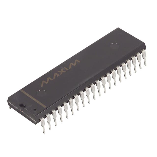
- Part No.:
- DS89C430-MNL
- Manufacturer:
- Analog Devices Inc./Maxim Integrated
- Category:
- Microcontrollers
- Package:
- 40-DIP (0.600", 15.24mm)
- Datasheet:
-
 DS89C430-MNL.pdf
- Description:
- IC MCU 8BIT 16KB FLASH 40DIP
- Quantity:
- Payment:

- Shipping:

Inventory:2,495
Please send an inquiry. Send us your inquiry, and we will respond immediately.
Product details
Overview
DS89C430-MNL from Maxim Integrated is a high-speed 8051-compatible flash microcontroller featuring a one-clock-per-machine-cycle core, 16kB on-chip flash memory, 1kB MOVX SRAM, and operation up to 33MHz (33 MIPS). It delivers up to 10× speed improvement over legacy 8051s at same crystal frequency and supports dual serial ports, five interrupt priority levels, and power-fail reset - deployed in industrial control, HVAC, and data logging systems.
For engineers reviewing the DS89C430-MNL datasheet, DS89C430-MNL pinout, DS89C430-MNL application, or DS89C430-MNL equivalent, key selection considerations include its 40-pin PDIP package, 33MHz max clock, 16kB flash size, ROMSIZE programmability, and compatibility with legacy 8051 codebases requiring timing recalibration.
Technical Context
The DS89C430-MNL implements a fully static CMOS 8051-compatible architecture with redesigned pipeline enabling single-cycle instruction execution - eliminating the 12-clock overhead of classic 8051s. Its clock system supports external crystal (1–33MHz) or clock input, with programmable dividers (up to 1024×) and optional crystal multipliers for flexible timing control.
It integrates dual data pointers with automatic increment/decrement/toggle select, four paged memory-access modes, and configurable MOVX access timing (2–9 machine cycles) to interface reliably with diverse external peripherals and memory devices across varying speed grades.
Key Specifications
| Parameter | Value and Actual Design Meaning |
|---|---|
| Core Architecture | High-speed 8051, one clock per machine cycle - enables 33 MIPS at 33MHz, eliminating legacy 12-cycle bottleneck. |
| Flash Memory | 16kB in-application programmable flash - supports field firmware updates via serial port without external programmer. |
| SRAM | 1kB dedicated MOVX SRAM - provides fast off-chip data access without external RAM latency penalties. |
| Max Clock Frequency | 33MHz system clock - achieves 30ns single-cycle instruction execution time for real-time deterministic response. |
| Operating Voltage | 4.5V to 5.5V - compatible with standard +5V industrial logic rails and brownout detection down to 3.95V reset threshold. |
| Temperature Range | -40°C to +85°C ambient - qualified for industrial and building automation environments without derating. |
| Power Modes | Active, Idle, and Stop modes with bandgap enable/disable - Stop mode draws ≤100µA (bandgap off) for ultra-low-power sleep. |
Pinout & Package
DS89C430-MNL is housed in a 40-pin Plastic Dual In-line Package (PDIP), with 0.6-inch body width and standard through-hole mounting. Pin spacing conforms to JEDEC MS-001, supporting legacy socketing and manual prototyping.
| Pin/Terminal | Circuit Role | Design Meaning |
|---|---|---|
| VCC (Pin 40) | Supply voltage input | +5V main power rail; decoupling required within 10mm for stable high-speed operation. |
| GND (Pin 20) | Logic ground reference | Primary return path for digital I/O and core logic; must be low-impedance connection to minimize noise coupling. |
| RST (Pin 9) | Reset input/output | Bidirectional Schmitt-triggered pin with internal 50–200kΩ pulldown - eliminates need for external RC network during power-up. |
| XTAL1 (Pin 19), XTAL2 (Pin 18) | Crystal oscillator interface | Supports fundamental-mode AT-cut crystals (1–33MHz); XTAL1 accepts external clock source when crystal omitted. |
| P0.0–P0.7 (Pins 39–32) | Multiplexed address/data bus (AD0–AD7) | Open-drain port requiring pullups when used as I/O; latches LSB address during ALE high for external memory interfacing. |
| P1.0–P1.7 (Pins 1–8) | General-purpose I/O with alternate functions | Includes T2/T2EX, RXD1/TXD1, and INT2–INT5 - enables hardware timer capture, second UART, and five edge-triggered interrupts. |
| P2.0–P2.7 (Pins 21–28) | Upper address bus (A8–A15) / I/O | Provides MSB address for external memory; supports page mode 1/2 addressing schemes for optimized memory access. |
| P3.0–P3.7 (Pins 10–17) | Multiplexed I/O with critical system functions | Hosts RXD0/TXD0, INT0/INT1, T0/T1, WR/RD - essential for serial communication, external event capture, and external RAM control. |
| EA (Pin 31) | External access select | Logic-high enables internal 16kB flash; grounded forces external program memory fetch - configurable per boot requirement. |
| ALE/PROG (Pin 30) | Address latch enable / programming mode | Generates strobe for external address latch (e.g., 74LS373); toggles to PROG mode for parallel flash programming. |
Key Features
| Feature | Design Value |
|---|---|
| Dual Data Pointers (DPTR/DPTR1) | Enables zero-overhead block memory moves between internal/external RAM; automatic increment/decrement reduces loop overhead by >40%. |
| ROMSIZE Programmability | Software-selectable internal program memory size (0–16kB) - allows dynamic remapping of external memory space without hardware change. |
| Variable MOVX Timing Control | MD2:MD0 bits configure MOVX access from 2–9 machine cycles - ensures reliable handshake with slow peripherals like EEPROM or LCD controllers. |
| EMI Reduction Mode | Disables ALE during idle periods - reduces radiated emissions by >15dB in sensitive building automation and medical equipment. |
| Power-Fail Warning & Reset | Dedicated VPFW (4.2–4.6V) and VRST (3.95–4.35V) thresholds - enables graceful shutdown and nonvolatile state save before brownout. |
Applications
| Industrial Control and Automation | HVAC System Controllers |
|---|---|
|
Use Scenario: Real-time monitoring and actuator control in PLC-based assembly lines with analog sensor inputs and relay outputs. IC Role / Device Role / Timing Role: Primary controller executing deterministic control loops at sub-millisecond intervals using Timer 0/1 and dual serial ports for Modbus RTU communication. Use Value: 33MHz execution speed ensures <100µs response to emergency stop signals, while 16kB flash accommodates safety-certified firmware and parameter tables. |
Use Scenario: Central air-handling unit (AHU) controller managing damper positions, fan speeds, and temperature setpoints across multiple zones. IC Role / Device Role / Timing Role: Main MCU coordinating RS-485 HVAC networks (via Serial Port 0), local CAN-like signaling (via P1.x GPIO), and analog-to-digital conversion timing. Use Value: Power-fail warning triggers backup battery switchover and logs last operational state to flash, preventing configuration loss during grid fluctuations. |
| Data Logging Systems | Building Energy Management |
|
Use Scenario: Standalone environmental logger recording temperature, humidity, and CO₂ every 10 seconds for 30 days using SD card or SPI FRAM. IC Role / Device Role / Timing Role: Host processor managing FAT32 file writes, RTC synchronization, and low-power sleep cycles via Stop mode and wake-on-interrupt. Use Value: 100µA Stop mode current extends battery life to >2 years on two AA cells; 1kB MOVX SRAM buffers sensor data during write latency. |
Use Scenario: Distributed BMS node aggregating lighting, occupancy, and power meter data for centralized dashboard visualization. IC Role / Device Role / Timing Role: Edge node performing local analytics (e.g., occupancy pattern recognition) and time-synchronized data transmission via Serial Port 1 to gateway. Use Value: Five interrupt priority levels isolate critical metering interrupts from UI polling, ensuring ±1ms timestamp accuracy for energy billing compliance. |
Equivalent & Alternatives
The following parts are listed as comparable options for similar 8051-compatible microcontroller applications.
| Alternative Part | Technical Difference | Application Difference | Selection Advice |
|---|---|---|---|
| DS89C450-MNL | 64kB flash (vs. 16kB), identical pinout, same speed/peripherals - drop-in replacement where larger firmware footprint is required. | Suitable for complex protocol stacks (e.g., BACnet/IP) or field-upgradable feature sets requiring >32kB code space. | Select DS89C450-MNL only if firmware exceeds 14kB after linker optimization; otherwise DS89C430-MNL offers better cost efficiency. |
| DS87C520 | Legacy 8051 derivative with 16kB flash but 12-clock-per-cycle core - ~3× slower at same crystal frequency; no ROMSIZE or dual DPTR. | Used in legacy designs where timing-critical ISR latency is relaxed and no new peripheral features (e.g., second UART) are needed. | Choose DS87C520 only for direct drop-in replacement in existing 8051 PCBs with unmodified timing-critical firmware; not recommended for new designs. |
Compared with DS89C450-MNL and DS87C520, DS89C430-MNL uniquely balances cost-effective 16kB flash capacity with ultra-high-speed execution and modern power management - making it optimal for mid-complexity industrial nodes where firmware size and real-time responsiveness are both constrained.
Availability
DS89C430-MNL is available at Aetrix Electronics and suitable for industrial control and automation, HVAC system controllers, and data logging systems requiring stable component supply and long-term manufacturability.
Supply support for DS89C430-MNL includes scheduled delivery planning, volume procurement assistance, BOM continuity management, traceable sourcing, and lifecycle availability coordination for OEM customers, industrial embedded developers, connected-device designers, and electronics production programs.
Manufacturer
Maxim Integrated (now part of Analog Devices) is a semiconductor company specializing in precision analog, mixed-signal, and high-reliability microcontrollers for industrial, automotive, and communications markets.
The DS89C430-MNL belongs to Maxim's Ultra-High-Speed Flash Microcontroller family, designed specifically to replace legacy 8051s in performance-constrained industrial applications while preserving software investment and board layout.
FAQ
What is the maximum operating frequency of the DS89C430-MNL?
The DS89C430-MNL supports a maximum system clock frequency of 33MHz, delivering 33 million instructions per second (MIPS) with single-cycle execution. This is achieved using an external crystal (1–33MHz) or clock source, with internal clock dividers/multipliers configured via the PMR register. At 33MHz, the fastest instructions execute in 30ns - verified across the full -40°C to +85°C industrial temperature range.
Does the DS89C430-MNL support in-system programming (ISP)?
Yes, the DS89C430-MNL supports in-system programming via its primary serial port (P3.0/P3.1) using ROM-resident or user-defined loader software. The 16kB flash memory can be reprogrammed without removing the device from the target board, enabling field firmware updates and configuration changes. Programming requires only standard UART-level signals and adheres to Maxim's documented ISP protocol.
How does the DS89C430-MNL handle power-fail conditions?
The DS89C430-MNL integrates dedicated circuitry for power-fail detection: VPFW (power-fail warning) triggers at 4.2–4.6V to initiate controlled shutdown, while VRST (reset trip point) asserts reset below 3.95–4.35V. This dual-threshold design allows firmware to save critical state to flash or external memory before reset occurs - a key requirement in data loggers and energy meters where data integrity is mandatory.
Is the DS89C430-MNL pin-compatible with standard 8051 microcontrollers?
Yes, the DS89C430-MNL is pin-compatible with standard 8051-family devices in the 40-pin PDIP package, including signal mapping for all four I/O ports, RST, XTAL1/XTAL2, EA, PSEN, ALE, RD, and WR. However, timing-critical firmware may require adjustment due to its 12× faster instruction execution - especially delay loops and baud rate generator calculations.
What memory resources are available on the DS89C430-MNL?
The DS89C430-MNL provides 16kB of on-chip flash memory for program storage, 256 bytes of standard 8051 scratchpad RAM, and 1kB of dedicated MOVX SRAM accessible via external data bus instructions. The ROMSIZE feature allows software to dynamically configure visible internal flash size (0–16kB), freeing the entire external address space for peripherals or additional memory when needed.
DS89C430-MNL Specifications
- Product attributes
- Attribute value
- Manufacturer:
- Analog Devices Inc./Maxim Integrated
- Package/Case:
- 40-DIP (0.600", 15.24mm)
- Series:
- 89C
- Packaging:
- Tube
- Product Status:
- Obsolete
- Programmable:
- Not Verified
- Core Processor:
- 8051
- Core Size:
- 8-Bit
- Speed:
- 33MHz
- Connectivity:
- EBI/EMI, SIO, UART/USART
- Peripherals:
- Power-Fail Reset, WDT
- Number of I/O:
- 32
- Program Memory Size:
- 16KB (16K x 8)
- Program Memory Type:
- FLASH
- EEPROM Size:
- -
- RAM Size:
- 1K x 8
- Voltage - Supply (Vcc/Vdd):
- 4.5V ~ 5.5V
- Data Converters:
- -
- Oscillator Type:
- External
- Operating Temperature:
- -40°C ~ 85°C (TA)
- Grade:
- -
- Qualification:
- -
- Mounting Type:
- Through Hole
- Supplier Device Package:
DS89C430-MNL FAQ
1.How can I place an order for DS89C430-MNL through Aetrix?
Please submit a Request for Quotation (RFQ) for DS89C430-MNL on Aetrix. Our sales agent will provide a competitive quotation and guide you through the order confirmation once you accept the terms.
2.Are the price and stock information for DS89C430-MNL reliable?
The price and inventory of DS89C430-MNL are updated periodically and may fluctuate due to market conditions. Stock and pricing data are typically refreshed every 24 hours. Quotation validity for DS89C430-MNL is usually 5 days.
3.What payment methods are accepted for DS89C430-MNL?
We accept Wire Transfer, PayPal, Credit Card, Western Union, MoneyGram, and Escrow for DS89C430-MNL transactions.
Note: Certain payment methods may incur a processing fee.
4.How is shipping managed for DS89C430-MNL?
DS89C430-MNL orders can be shipped via leading logistics carriers, including DHL, UPS, FedEx, TNT, or Registered Mail.
Once your DS89C430-MNL order is processed, you will receive an email with the shipment details and tracking number.
Note: Tracking information may take up to 24 hours to appear. Express delivery typically takes 3–5 business days.
5.How can I obtain technical support or documentation for DS89C430-MNL?
For technical support, including DS89C430-MNL datasheets, pinout diagrams, or application guidance, please contact our engineering support team. They can provide detailed documentation and assistance for your DS89C430-MNL requirements.
6.How does Aetrix verify that DS89C430-MNL is sourced from the original manufacturer or authorized distributors?
All DS89C430-MNL products on Aetrix are procured from qualified distributors and authorized channels. Our dedicated quality assurance team conducts strict verification, including traceability checks and, if necessary, third-party testing. This ensures that DS89C430-MNL meets industry standards.
7.What is the process for return or replacement of DS89C430-MNL?
All DS89C430-MNL units undergo pre-shipment inspection (PSI). If there is an issue with DS89C430-MNL, returns or replacements are accepted under the following conditions:
1.Quantity discrepancies, incorrect items, or visible external defects (such as breakage or corrosion), acknowledged by Aetrix.
2.The issue is reported within 90 days of delivery.
3.The DS89C430-MNL part is unused and in its original packaging.
Return procedure for DS89C430-MNL:
1.Submit a request within 90 days.
2.Obtain a Return Material Authorization (RMA) from Aetrix.
DS89C430-MNL Tags

-
ATTINY4-TSHR
Microchip Technology
-
ATTINY10-TSHR
Microchip Technology
-
ATTINY10-TS8R
Microchip Technology

-
ATTINY202-SSNR
Microchip Technology
-
ATTINY202-SSFR
Microchip Technology
-
ATTINY402-SSNR
Microchip Technology

-
PIC16F15213T-I/MF
Microchip Technology
-
PIC16F15213-E/MF
Microchip Technology

-
PIC10F200T-I/OT
Microchip Technology
-
ATTINY412-SSNR
Microchip Technology
-
PIC10F202T-I/OT
Microchip Technology

-
ATTINY404-SSNR
Microchip Technology
Tech Hub

A practical engineering guide to 3.3V and 5V logic compatibility, input thresholds, resistor dividers, translator ICs, MOSFET level shifting, I2C pull-ups, timing limits and power-sequencing risks.

The 74HC595 uses push-pull logic outputs, while the TPIC6B595 uses 50 V open-drain DMOS sinks for higher-power loads. This guide compares timing, current limits, 3.3 V interfacing, load wiring, thermal…

The 74HC595 converts serial data into eight stable parallel outputs. This guide covers pin functions, shift and storage timing, OE and MR behavior, drive-current limits, cascading, voltage compatibilit…

A technical comparison of level-sensitive latches and edge-triggered flip-flops, covering timing windows, setup and hold limits, master–slave operation, time borrowing, race-through, HDL inference and…

A D latch stores one bit while Enable controls when data can pass. This reference covers gate-level operation, truth tables, transparency, setup and hold timing, LE versus OE, common ICs and practical …

An SR latch stores one bit through cross-coupled feedback. This engineering reference covers NOR and NAND implementations, truth tables, forbidden-state recovery, gated operation, switch debouncing, fa…

Latch circuits retain one bit through feedback. This technical reference covers SR and D latches, truth tables, transparency, timing limits, latch-versus-flip-flop behavior, applications and common log…

An engineering guide to LED driver operation, constant-current and constant-voltage outputs, linear and switching topologies, dimming, IC selection, calculations, replacement compatibility, and fault c…

Operational amplifier guide covering op amp basics, feedback, ideal vs real op amps, common configurations, buffer circuits, offset, bias current, gain-bandwidth, slew rate, rail-to-rail limits and sel…

Jumper cables guide covering safe connection order, red and black clamp placement, final ground connection, cable gauge, length, clamp quality, copper vs CCA cables, jump starter comparison and battery…


