
 My Inquiry
 My Account


Analog Devices Inc./Maxim Integrated DS89C450-MNG+
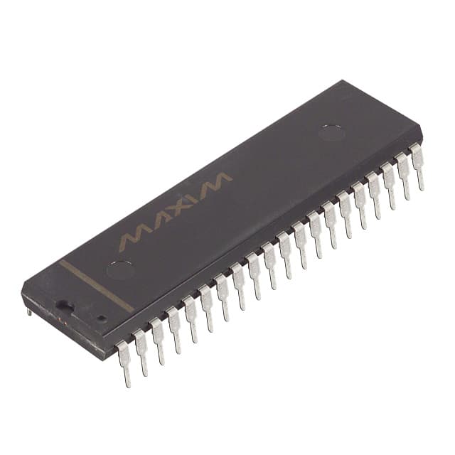
- Part No.:
- DS89C450-MNG+
- Manufacturer:
- Analog Devices Inc./Maxim Integrated
- Category:
- Microcontrollers
- Package:
- 40-DIP (0.600", 15.24mm)
- Datasheet:
-
 DS89C450-MNG+.pdf
- Description:
- IC MCU 8BIT 64KB FLASH 40DIP
- Quantity:
- Payment:

- Shipping:

Inventory:4,678
Please send an inquiry. Send us your inquiry, and we will respond immediately.
Product details
Overview
DS89C450-MNG+ from Maxim Integrated is a 64kB flash, 40-pin PDIP-packaged, ultra-high-speed 8051-compatible microcontroller executing instructions at 1 clock per machine cycle, supporting up to 33MHz system clock (33 MIPS), with dual serial ports, 1kB MOVX SRAM, and programmable power management. It serves in industrial control, data logging, and white goods where deterministic real-time response and in-system reprogrammability are required.
For engineers reviewing the DS89C450-MNG+ datasheet, DS89C450-MNG+ pinout, DS89C450-MNG+ application, or DS89C450-MNG+ equivalent, key selection criteria include flash size (64kB), 40-pin PDIP package compatibility with legacy 8051 sockets, single-cycle execution timing, ROMSIZE configurability, and dual full-duplex UART support for embedded telemetry and control interfaces.
Technical Context
The DS89C450-MNG+ implements a redesigned 8051 core with one-clock-per-instruction execution, eliminating the traditional 12-clock-per-cycle bottleneck. Its architecture supports five interrupt priority levels, seven external interrupt sources (INT0–INT5 plus power-fail), and variable-length MOVX access with up to 9-cycle stretch for external memory timing alignment.
It integrates dual hardware serial ports (UART0 and UART1), a programmable watchdog timer, early-warning power-fail interrupt, and ROMSIZE register enabling dynamic selection of internal program memory size (0–64kB) while preserving full external address map access - critical for hybrid memory architectures in field-upgradable systems.
Key Specifications
| Parameter | Value and Actual Design Meaning |
|---|---|
| Core Architecture | High-speed 8051, 1 clock per machine cycle - enables 33 MIPS at 33MHz, 12× faster than legacy 8051 at same crystal frequency |
| Flash Memory | 64kB on-chip, in-application programmable via serial port - supports firmware updates without chip removal or external programmer |
| SRAM | 1kB dedicated MOVX RAM - provides fast external-data-bus-accessible buffer space for DMA-like block transfers using dual DPTRs |
| Max System Clock | 33MHz - delivers 33 million instructions per second with guaranteed operation across -40°C to +85°C ambient range |
| Supply Voltage | 4.5V to 5.5V - compatible with standard 5V industrial logic rails and tolerant of brownout conditions down to VRST = 3.95V |
| Power Modes | Active/Idle/Stop with bandgap on/off - Stop mode draws ≤100µA (bandgap disabled), enabling battery-backed low-power monitoring |
| Serial Interfaces | Two full-duplex UARTs - UART0 (P3.0/P3.1) and UART1 (P1.2/P1.3) support independent baud rates and simultaneous host/peripheral communication |
Pinout & Package
DS89C450-MNG+ uses a 40-pin Plastic Dual In-line Package (PDIP) with 0.6-inch body width, RoHS-compliant lead-free finish, and standard 0.1-inch pin pitch - directly socket-compatible with legacy 8051-based PCB footprints.
| Pin/Terminal | Circuit Role | Design Meaning |
|---|---|---|
| VCC (Pin 40) | Primary power supply | +5V supply input; must be decoupled locally with ≥0.1µF ceramic capacitor to meet 33MHz switching noise requirements |
| GND (Pin 20) | Logic ground reference | Common return path for all digital I/O and core logic; requires low-impedance connection to PCB ground plane |
| RST (Pin 9) | Reset input/output | Bidirectional Schmitt-triggered reset pin with internal 50–200kΩ pulldown - eliminates need for external RC network during power-up |
| XTAL1 (Pin 19), XTAL2 (Pin 18) | Clock oscillator interface | Supports fundamental-mode AT-cut crystals (1–33MHz) or external CMOS clock source; XTAL1 accepts direct clock input when crystal omitted |
| P0.0–P0.7 (Pins 39–32) | Multiplexed address/data bus | Open-drain port with weak pullups; outputs LSB address during ALE high, transitions to bidirectional data bus on ALE low - requires external pullups for I/O use |
| P2.0–P2.7 (Pins 21–28) | Upper address bus / I/O | Provides A8–A15 during external memory access; functions as general-purpose I/O otherwise - retains weak pullup in reset state |
| P3.6 (WR), P3.7 (RD) | External memory strobes | Active-low write/read control signals synchronized to ALE - drive external RAM/peripherals in expanded memory configurations |
| EA (Pin 31) | External access select | High = execute from internal 64kB flash; low = fetch code from external memory - enables seamless transition between embedded and external program storage |
Key Features
| Feature | Design Value |
|---|---|
| Dual Data Pointers (DPTR/DPTR1) | Enables zero-overhead block memory moves between internal/external RAM; automatic increment/decrement and toggle select reduce instruction count in data transfer loops |
| ROMSIZE Register | Software-configurable internal program memory size (0–64kB); allows runtime partitioning of flash for bootloader/application separation without hardware change |
| Variable-Length MOVX Timing | MD2:MD0 bits add 2–9 machine cycles of wait states to MOVX reads/writes - matches timing to slow peripherals (e.g., LCD controllers, EEPROMs) without CPU polling |
| EMI Reduction Mode | Disables ALE output during idle periods - reduces radiated emissions by eliminating unnecessary clock harmonics in noise-sensitive environments like medical or automotive systems |
| Power-Fail Detection | Integrated comparator triggers early-warning interrupt at VPFW = 4.2–4.6V and hard reset at VRST = 3.95–4.35V - enables graceful shutdown and nonvolatile state save before brownout |
Applications
| Data Logging Systems | Industrial HVAC Controllers |
|---|---|
Use Scenario: Standalone environmental sensor node recording temperature, humidity, and energy consumption at 1Hz intervals onto SD card or internal flash. IC Role / Device Role: Primary controller managing sensor I²C/SPI interfaces, SD card FAT32 file writes, real-time clock synchronization, and USB/UART telemetry upload. Use Value: 64kB flash stores multi-week log history; dual UARTs enable concurrent local debug (UART0) and remote cloud upload (UART1); 33 MIPS handles CRC-32 computation and timestamping in real time. |
Use Scenario: Zone-level HVAC unit regulating fan speed, damper position, and compressor staging based on occupancy and ambient sensors. IC Role / Device Role: Real-time motion- and CO₂-triggered actuator coordinator interfacing with PWM fan drivers, analog temperature inputs, and RS-485 BACnet gateway. Use Value: ROMSIZE register isolates bootloader from application firmware for safe over-the-air updates; programmable watchdog ensures recovery from sensor fault lockups; 1kB MOVX RAM buffers PID loop coefficients and setpoint history. |
| White Goods Control Boards | Uninterruptible Power Supplies (UPS) |
Use Scenario: Washing machine main control board managing motor phase sequencing, water valve timing, temperature ramping, and user interface display. IC Role / Device Role: Central sequencer coordinating TRIAC-driven heater control, brushless DC motor commutation via external gate driver, and touch-button debounce logic. Use Value: Single-cycle execution meets <50µs motor commutation timing deadlines; dual serial ports support factory programming (UART0) and service diagnostics (UART1); power-fail interrupt initiates emergency spin-down before AC loss. |
Use Scenario: Line-interactive UPS monitoring AC input voltage, battery charge state, and load current while managing inverter switching and relay transfer logic. IC Role / Device Role: Safety-critical supervisor executing ADC sampling, battery protection algorithms, and failover decision tree with <10ms response latency. Use Value: Early-warning power-fail interrupt triggers battery switchover at 4.375V threshold; stop-mode current ≤100µA extends backup runtime during standby; 33MHz clock ensures 12-bit ADC conversion + calculation completes within 200µs window. |
Equivalent & Alternatives
The following parts are listed as comparable options for similar 8051-compatible microcontroller applications.
| Alternative Part | Technical Difference | Application Difference | Selection Advice |
|---|---|---|---|
| DS89C430-MNL+ | 16kB flash (vs. 64kB), identical 40-pin PDIP package, same core speed and peripheral set | Suitable for cost-sensitive designs with smaller firmware footprints; lacks capacity for complex GUI or protocol stacks | Select when firmware size ≤14kB and no future feature expansion is planned |
| DS87C520-QCL+ | 32kB flash, 44-PLCC package, 33MHz max, but 4-cycle-per-instruction core (vs. 1-cycle) | Lower performance (≤8.25 MIPS at 33MHz); requires PCB redesign due to different pinout and package | Choose only if legacy PLCC footprint is fixed and 8 MIPS suffices for control tasks |
Compared with DS89C430-MNL+ and DS87C520-QCL+, the DS89C450-MNG+ delivers 4× more flash than the former and 4× higher instruction throughput than the latter - making it optimal for field-upgradable, feature-rich embedded controllers where code density and real-time determinism are critical.
Availability
DS89C450-MNG+ is available at Aetrix Electronics and suitable for industrial control, data logging, and white goods applications requiring stable component supply, long-term lifecycle support, and RoHS-compliant manufacturing.
Supply support for DS89C450-MNG+ includes scheduled delivery planning, volume procurement assistance, BOM continuity management, traceable sourcing, and lifecycle availability coordination for OEM customers, industrial embedded developers, connected-device designers, and electronics production programs.
Manufacturer
Maxim Integrated (now part of Analog Devices) is a semiconductor company specializing in precision analog, mixed-signal, and high-reliability microcontrollers for industrial, medical, and communications markets.
The DS89C450-MNG+ belongs to Maxim's Ultra-High-Speed Flash Microcontroller family, designed specifically to replace legacy 8051s in performance-constrained embedded systems while maintaining full software and pin compatibility.
FAQ
What is the maximum operating frequency of the DS89C450-MNG+?
The DS89C450-MNG+ supports a maximum system clock frequency of 33MHz, delivering 33 million instructions per second (MIPS) with its one-clock-per-instruction architecture. This is validated across the full industrial temperature range (-40°C to +85°C) and supply voltage (4.5V to 5.5V). The DS89C450-MNG+ achieves this performance using either an external crystal (1–33MHz) or CMOS clock source, with internal clock dividers and multipliers configurable via the PMR register.
Does the DS89C450-MNG+ support in-system programming (ISP)?
Yes, the DS89C450-MNG+ supports in-system programming via its primary UART (P3.0/P3.1) using the built-in ROM-resident bootloader. Firmware updates can be performed without removing the device from the PCB or using external programming hardware. The DS89C450-MNG+ also supports parallel programming for high-volume manufacturing using industry-standard programmers, leveraging the ALE/PROG pin functionality.
How does the power-fail detection feature work on the DS89C450-MNG+?
The DS89C450-MNG+ integrates two voltage comparators: one triggers an early-warning interrupt at VPFW = 4.2–4.6V, and another asserts hardware reset at VRST = 3.95–4.35V. This staged response allows firmware running on the DS89C450-MNG+ to save critical state, disable actuators, and initiate controlled shutdown before supply collapse. The internal pulldown on RST eliminates external components, and the guaranteed voltage separation prevents metastability.
Can the DS89C450-MNG+ replace a standard 8051 in an existing design?
Yes, the DS89C450-MNG+ is pin-compatible and instruction-set-compatible with standard 8051 microcontrollers in the 40-pin PDIP package. It operates at the same VCC/GND pins, shares identical I/O port structure (P0–P3), and maintains compatibility with legacy peripherals and development tools. However, timing-critical code may require adjustment due to its 12× faster execution - the DS89C450-MNG+ defaults timers to 12-cycle mode for backward compatibility unless explicitly reconfigured.
What memory resources are available on the DS89C450-MNG+?
The DS89C450-MNG+ integrates 64kB of on-chip flash memory for program storage, 256 bytes of standard 8051 scratchpad RAM, and 1kB of dedicated MOVX-accessible SRAM for external-data-bus operations. The ROMSIZE register allows dynamic configuration of active internal program memory size (0–64kB), enabling flexible memory mapping for bootloader/application separation or hybrid internal/external code execution - all managed in software without hardware modification.
DS89C450-MNG+ Specifications
- Product attributes
- Attribute value
- Manufacturer:
- Analog Devices Inc./Maxim Integrated
- Package/Case:
- 40-DIP (0.600", 15.24mm)
- Series:
- 89C
- Packaging:
- Tube
- Product Status:
- Obsolete
- Programmable:
- Not Verified
- Core Processor:
- 8051
- Core Size:
- 8-Bit
- Speed:
- 25MHz
- Connectivity:
- EBI/EMI, SIO, UART/USART
- Peripherals:
- Power-Fail Reset, WDT
- Number of I/O:
- 32
- Program Memory Size:
- 64KB (64K x 8)
- Program Memory Type:
- FLASH
- EEPROM Size:
- -
- RAM Size:
- 1K x 8
- Voltage - Supply (Vcc/Vdd):
- 4.5V ~ 5.5V
- Data Converters:
- -
- Oscillator Type:
- External
- Operating Temperature:
- -40°C ~ 85°C (TA)
- Grade:
- -
- Qualification:
- -
- Mounting Type:
- Through Hole
- Supplier Device Package:
DS89C450-MNG+ FAQ
1.How can I place an order for DS89C450-MNG+ through Aetrix?
Please submit a Request for Quotation (RFQ) for DS89C450-MNG+ on Aetrix. Our sales agent will provide a competitive quotation and guide you through the order confirmation once you accept the terms.
2.Are the price and stock information for DS89C450-MNG+ reliable?
The price and inventory of DS89C450-MNG+ are updated periodically and may fluctuate due to market conditions. Stock and pricing data are typically refreshed every 24 hours. Quotation validity for DS89C450-MNG+ is usually 5 days.
3.What payment methods are accepted for DS89C450-MNG+?
We accept Wire Transfer, PayPal, Credit Card, Western Union, MoneyGram, and Escrow for DS89C450-MNG+ transactions.
Note: Certain payment methods may incur a processing fee.
4.How is shipping managed for DS89C450-MNG+?
DS89C450-MNG+ orders can be shipped via leading logistics carriers, including DHL, UPS, FedEx, TNT, or Registered Mail.
Once your DS89C450-MNG+ order is processed, you will receive an email with the shipment details and tracking number.
Note: Tracking information may take up to 24 hours to appear. Express delivery typically takes 3–5 business days.
5.How can I obtain technical support or documentation for DS89C450-MNG+?
For technical support, including DS89C450-MNG+ datasheets, pinout diagrams, or application guidance, please contact our engineering support team. They can provide detailed documentation and assistance for your DS89C450-MNG+ requirements.
6.How does Aetrix verify that DS89C450-MNG+ is sourced from the original manufacturer or authorized distributors?
All DS89C450-MNG+ products on Aetrix are procured from qualified distributors and authorized channels. Our dedicated quality assurance team conducts strict verification, including traceability checks and, if necessary, third-party testing. This ensures that DS89C450-MNG+ meets industry standards.
7.What is the process for return or replacement of DS89C450-MNG+?
All DS89C450-MNG+ units undergo pre-shipment inspection (PSI). If there is an issue with DS89C450-MNG+, returns or replacements are accepted under the following conditions:
1.Quantity discrepancies, incorrect items, or visible external defects (such as breakage or corrosion), acknowledged by Aetrix.
2.The issue is reported within 90 days of delivery.
3.The DS89C450-MNG+ part is unused and in its original packaging.
Return procedure for DS89C450-MNG+:
1.Submit a request within 90 days.
2.Obtain a Return Material Authorization (RMA) from Aetrix.
DS89C450-MNG+ Tags

-
ATTINY4-TSHR
Microchip Technology
-
ATTINY10-TSHR
Microchip Technology
-
ATTINY10-TS8R
Microchip Technology

-
ATTINY202-SSNR
Microchip Technology
-
ATTINY202-SSFR
Microchip Technology
-
ATTINY402-SSNR
Microchip Technology

-
PIC16F15213T-I/MF
Microchip Technology
-
PIC16F15213-E/MF
Microchip Technology

-
PIC10F200T-I/OT
Microchip Technology
-
ATTINY412-SSNR
Microchip Technology
-
PIC10F202T-I/OT
Microchip Technology

-
ATTINY404-SSNR
Microchip Technology
Tech Hub

A practical engineering guide to 3.3V and 5V logic compatibility, input thresholds, resistor dividers, translator ICs, MOSFET level shifting, I2C pull-ups, timing limits and power-sequencing risks.

The 74HC595 uses push-pull logic outputs, while the TPIC6B595 uses 50 V open-drain DMOS sinks for higher-power loads. This guide compares timing, current limits, 3.3 V interfacing, load wiring, thermal…

The 74HC595 converts serial data into eight stable parallel outputs. This guide covers pin functions, shift and storage timing, OE and MR behavior, drive-current limits, cascading, voltage compatibilit…

A technical comparison of level-sensitive latches and edge-triggered flip-flops, covering timing windows, setup and hold limits, master–slave operation, time borrowing, race-through, HDL inference and…

A D latch stores one bit while Enable controls when data can pass. This reference covers gate-level operation, truth tables, transparency, setup and hold timing, LE versus OE, common ICs and practical …

An SR latch stores one bit through cross-coupled feedback. This engineering reference covers NOR and NAND implementations, truth tables, forbidden-state recovery, gated operation, switch debouncing, fa…

Latch circuits retain one bit through feedback. This technical reference covers SR and D latches, truth tables, transparency, timing limits, latch-versus-flip-flop behavior, applications and common log…

An engineering guide to LED driver operation, constant-current and constant-voltage outputs, linear and switching topologies, dimming, IC selection, calculations, replacement compatibility, and fault c…

Operational amplifier guide covering op amp basics, feedback, ideal vs real op amps, common configurations, buffer circuits, offset, bias current, gain-bandwidth, slew rate, rail-to-rail limits and sel…

Jumper cables guide covering safe connection order, red and black clamp placement, final ground connection, cable gauge, length, clamp quality, copper vs CCA cables, jump starter comparison and battery…


