
 My Inquiry
 My Account


Texas Instruments DS90C185SQ/NOPB
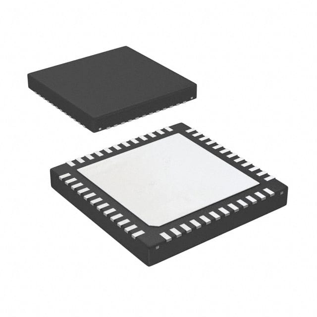
- Part No.:
- DS90C185SQ/NOPB
- Manufacturer:
- Texas Instruments
- Category:
- Serializers, Deserializers
- Package:
- 48-WFQFN Exposed Pad
- Datasheet:
-
 DS90C185SQ/NOPB.pdf
- Description:
- IC SERIALIZER LVDS LP 48WQFN
- Quantity:
- Payment:

- Shipping:

Inventory:872
Please send an inquiry. Send us your inquiry, and we will respond immediately.
Product details
Overview
DS90C185SQ/NOPB from Texas Instruments is a low-power 1.8-V LVCMOS-to-LVDS serializer for portable display interfaces, supporting SXGA+ (1400×1050@60 Hz) resolution with 24-bit RGB + 3 control signals (HS/VS/DE), 25–105 MHz pixel clock range, and 4D+C (4 data lanes + clock) FPD-Link output. It serves as the GPU-side transmitter in compact LCD modules for media tablets and netbooks.
For engineers reviewing the DS90C185SQ/NOPB datasheet, DS90C185SQ/NOPB pinout, DS90C185SQ/NOPB application, or DS90C185SQ/NOPB equivalent, key selection criteria include 1.8-V single-supply operation, 24-/18-bit RGB mode configurability via 18B_MODE, LVDS VOD select (±180 mV / ±300 mV), sleep-mode power-down (PDB), and WQFN-48 package compatibility with high-density portable layouts.
Technical Context
The DS90C185SQ/NOPB implements a parallel-to-serial conversion architecture with integrated PLL, accepting 28-bit LVCMOS inputs (24 RGB + 3 video control + 1 GP/L-R) and serializing them into four differential LVDS data lanes (TxOUT0–3) plus TxCLKOUT. Its dual-mode operation-24-bit (4D+C) or 18-bit (3D+C)-is controlled by the 18B_MODE pin, which tri-states TxOUT3 in 18-bit mode to reduce power.
Timing is synchronized to an external pixel clock (25–105 MHz); data latching edge (rising/falling) is configurable via RFB pin. The serializer supports spread-spectrum clocking and achieves ≤0.035 UI cycle-to-cycle jitter at 105 MHz, with propagation delay of 10.54–13.96 ns and channel-to-channel skew ≤110 ps.
Key Specifications
| Parameter | Value and Actual Design Meaning |
|---|---|
| Supply Voltage | 1.71–1.89 V - Single 1.8-V rail powers core, I/O, and PLL; enables ultra-low-power portable design. |
| Pixel Clock Range | 25–105 MHz - Supports resolutions from VGA to SXGA+ (1400×1050@60 Hz) with scalable bandwidth. |
| Throughput | 2.94 Gbps max - Achieved at 105 MHz × 28 bits; enables full 24-bit RGB video transmission over LVDS. |
| LVDS Output VOD | ±180 mV (low-power) or ±300 mV (long-cable) - Configurable via VOD_SEL pin for trace/cable length optimization. |
| Power Dissipation | 50 mW typical at 75-MHz pclk - Enabled by 1.8-V LVCMOS design and sleep mode (PDB). |
| Operating Temp | −10°C to +70°C - Qualified for commercial portable electronics environments. |
| Package | 48-pin WQFN (6 mm × 6 mm × 0.8 mm) - Small footprint with exposed thermal pad (DAP = GND) for thermal management. |
Pinout & Package
DS90C185SQ/NOPB uses a 48-pin WQFN package (TI package code NJV) with 0.4-mm pitch and thermally enhanced DAP (die attach pad) connected to GND. Pinout includes 28 LVCMOS inputs (D0–D27), 10 LVDS outputs (TxOUT0–3±, TxCLKOUT±), 5 control inputs (RFB, 18B_MODE, VOD_SEL, PDB, CLK), and 5 power/ground terminals (VDD, VDDTX, VDDPLL, GND×2).
| Pin/Terminal | Circuit Role | Design Meaning |
|---|---|---|
| D0–D27 | LVCMOS parallel data input | 28-bit bus: 8R/8G/8B + HSync/VSync/DE + GP bit; all 1.8-V tolerant with internal pull-downs. |
| CLK | LVCMOS pixel clock input | 25–105 MHz timing reference; latching edge selected by RFB pin (rising/falling). |
| TxOUT0–3±, TxCLKOUT± | LVDS differential outputs | 4 data lanes + clock (4D+C); each pair requires 100-Ω differential termination; TxOUT3 tri-stated in 18-bit mode. |
| RFB | LVCMOS strobe edge select | Configures CLK edge sampling: 0 = falling edge (default), 1 = rising edge. |
| 18B_MODE | RGB depth mode control | 0 = 24-bit RGB (4D+C active), 1 = 18-bit RGB (3D+C, TxOUT3 disabled). |
| VOD_SEL | VOD level select | 0 = ±180 mV (low-power), 1 = ±300 mV (higher noise margin/longer traces). |
| PDB | Power-down bar input | Active-high; 0 = sleep mode (≤200 µA IDDZ), 1 = active (full functionality). |
| VDD / VDDTX / VDDPLL | Power supply rails | VDD (digital core), VDDTX (LVDS drivers), VDDPLL (PLL); each requires dedicated 0.1-µF bypass + VDDPLL needs 4.7–22-µF bulk cap. |
Key Features
| Feature | Design Value |
|---|---|
| Single 1.8-V supply operation | Eliminates multi-rail power design complexity and reduces BOM count in battery-powered systems. |
| Configurable 24-/18-bit RGB mode | Reduces LVDS lane count and dynamic power by 25% in 18-bit applications without changing PCB layout. |
| Selectable LVDS output voltage swing | Enables trade-off between EMI/noise immunity (±300 mV) and power savings (±180 mV) per system requirements. |
| Hardware sleep mode (PDB) | Reduces quiescent current to ≤200 µA, extending battery life during display idle periods in tablets and e-readers. |
| Integrated PLL with fast lock time | PLL set time ≤1 ms ensures rapid display initialization after wake-up, minimizing black-screen duration. |
Applications
| eBook Display Interface | Media Tablet GPU Link |
|---|---|
Use Scenario: Driving 1024×768 or 1280×800 e-ink or low-power LCD panels from ARM-based SoC GPU outputs. IC Role / Device Role / Timing Role: LVCMOS-to-LVDS serializer converting parallel RGB interface to noise-immune 4D+C FPD-Link for panel connection. Use Value: Enables 1.8-V-only system design, cuts interconnect EMI vs. parallel RGB, and supports deep-sleep power states via PDB pin. | Use Scenario: Transmitting SXGA+ (1400×1050) video from application processor to high-resolution display module in Android/iOS tablets. IC Role / Device Role / Timing Role: High-speed serializer synchronizing to 105-MHz pixel clock with <110-ps channel skew for accurate color timing. Use Value: Delivers 2.94 Gbps throughput with <0.035 UI jitter, ensuring clean image rendering and eliminating visible artifacts at full resolution. |
| Netbook Main Display Driver | Portable Monitor Control Board |
Use Scenario: Replacing legacy parallel RGB interface in thin-and-light x86 netbooks with compact LVDS-based display subsystems. IC Role / Device Role / Timing Role: Serializer bridging GPU's 24-bit LVCMOS output to 4D+C LVDS input of TCON (timing controller) on display module. Use Value: Reduces PCB routing layers and connector pin count by >60%, enabling thinner chassis and lower assembly cost. | Use Scenario: Integrating into USB-C or miniDP-to-LVDS adapter boards for external portable monitors up to 1400×1050. IC Role / Device Role / Timing Role: Fixed-function serializer providing deterministic latency and robust LVDS drive for plug-and-play monitor compatibility. Use Value: Supports spread-spectrum clocking and 100-Ω differential termination compliance, meeting EMI standards for Class B computing devices. |
Equivalent & Alternatives
The following parts are listed as comparable options for similar LVDS serializer applications.
| Alternative Part | Technical Difference | Application Difference | Selection Advice |
|---|---|---|---|
| DS90C187SQ/NOPB | Same 48-pin WQFN package and pinout; supports identical 24-/18-bit modes but adds programmable input mapping (MSB/LSB on CH3) and enhanced spread-spectrum support. | Preferred when flexible color data alignment or tighter EMI control is required across multiple display vendors. | Select DS90C187SQ/NOPB if input data mapping must be reconfigured without hardware change; otherwise DS90C185SQ/NOPB offers lower cost and simpler layout. |
| SN65LVDS31IPW | 5-channel LVDS transmitter (4D+C) without serialization logic; requires external parallel-to-serial logic; operates at 3.3 V, not 1.8 V. | Suitable only in systems with existing 3.3-V infrastructure and FPGA/CPLD-based pixel formatting. | Choose SN65LVDS31IPW only if migrating legacy 3.3-V designs; DS90C185SQ/NOPB is mandatory for new 1.8-V portable architectures. |
Compared with DS90C187SQ/NOPB, DS90C185SQ/NOPB provides identical core serialization and power features at lower cost and reduced configuration overhead; versus SN65LVDS31IPW, it integrates full parallel-to-serial conversion and 1.8-V operation-eliminating external logic and voltage translation in modern portable designs.
Availability
DS90C185SQ/NOPB is available at Aetrix Electronics and suitable for media tablet displays, netbook main screens, and portable monitor control boards requiring stable component supply, RoHS-compliant packaging, and long-term industrial availability.
Supply support for DS90C185SQ/NOPB includes scheduled delivery planning, volume procurement assistance, BOM continuity management, traceable sourcing, and lifecycle availability coordination for OEM customers, industrial embedded developers, connected-device designers, and electronics production programs.
Manufacturer
Texas Instruments is a global semiconductor leader specializing in analog, embedded processing, and connectivity technologies for industrial, automotive, and consumer applications.
The DS90C185SQ/NOPB belongs to TI's FPD-Link serializer product line, engineered specifically for low-power, high-resolution display interfaces in portable electronics where size, thermal performance, and single-supply simplicity are critical.
FAQ
What is the primary function of the DS90C185SQ/NOPB in a display system?
The DS90C185SQ/NOPB functions as an LVCMOS-to-LVDS serializer that converts a 28-bit parallel video interface (24-bit RGB + HSync/VSync/DE) into a 4D+C (four data lanes + clock) FPD-Link LVDS stream. It sits between the GPU and display TCON, enabling high-speed, low-noise, low-power transmission over compact flex cables in portable devices. DS90C185SQ/NOPB supports both 24-bit and 18-bit RGB modes with hardware-configurable pins.
Does DS90C185SQ/NOPB support both 24-bit and 18-bit RGB color depths?
Yes, DS90C185SQ/NOPB supports both 24-bit RGB (4D+C mode) and 18-bit RGB (3D+C mode) via the 18B_MODE pin. When 18B_MODE = 0, all four LVDS data lanes operate; when 18B_MODE = 1, TxOUT3± is tri-stated and corresponding inputs are ignored, reducing power consumption by ~25%. DS90C185SQ/NOPB maintains identical pinout and timing behavior in both modes.
How does the PDB pin affect power consumption in DS90C185SQ/NOPB?
The PDB (Power Down Bar) pin places DS90C185SQ/NOPB into a low-power sleep state when driven LOW, reducing supply current to ≤200 µA. In this mode, the PLL shuts down, LVDS drivers are powered off and pulled to GND via 100-Ω resistors, and all outputs become high-impedance. DS90C185SQ/NOPB resumes full operation within 100 ns after PDB is asserted HIGH.
What LVDS load impedance does DS90C185SQ/NOPB require?
DS90C185SQ/NOPB requires a nominal 100-Ω differential load on each LVDS output pair (TxOUT0–3± and TxCLKOUT±), with acceptable range of 80–120 Ω. This matches ANSI/TIA/EIA-644-A LVDS receiver specifications and ensures signal integrity, proper common-mode rejection, and minimal reflections. Termination must be placed at the display-side receiver end.
Can DS90C185SQ/NOPB operate with a 25-MHz pixel clock for VGA resolution?
Yes, DS90C185SQ/NOPB supports pixel clock frequencies from 25 MHz to 105 MHz, making it fully compatible with VGA (640×480@60 Hz, ~25.2 MHz) and higher resolutions including SXGA+ (1400×1050@60 Hz, ~105 MHz). At 25 MHz, DS90C185SQ/NOPB delivers 700 Mbps total throughput (28 bits × 25 MHz) while maintaining sub-110-ps channel skew and <0.035 UI jitter.
DS90C185SQ/NOPB Specifications
- Product attributes
- Attribute value
- Manufacturer:
- Texas Instruments
- Series:
- -
- Package/Case:
- 48-WFQFN Exposed Pad
- Packaging:
- Tape & Reel (TR)
- Product Status:
- Active
- Function:
- Serializer
- Data Rate:
- 2.94Gbps
- Input Type:
- LVCMOS
- Output Type:
- FPD-Link, LVDS
- Number of Inputs:
- 28
- Number of Outputs:
- 4
- Voltage - Supply:
- 1.71V ~ 1.89V
- Operating Temperature:
- -10°C ~ 70°C (TA)
- Grade:
- Automotive
- Qualification:
- AEC-Q100
- Mounting Type:
- Surface Mount
- Supplier Device Package:
- 48-WQFN (6x6)
DS90C185SQ/NOPB FAQ
1.How can I place an order for DS90C185SQ/NOPB through Aetrix?
Please submit a Request for Quotation (RFQ) for DS90C185SQ/NOPB on Aetrix. Our sales agent will provide a competitive quotation and guide you through the order confirmation once you accept the terms.
2.Are the price and stock information for DS90C185SQ/NOPB reliable?
The price and inventory of DS90C185SQ/NOPB are updated periodically and may fluctuate due to market conditions. Stock and pricing data are typically refreshed every 24 hours. Quotation validity for DS90C185SQ/NOPB is usually 5 days.
3.What payment methods are accepted for DS90C185SQ/NOPB?
We accept Wire Transfer, PayPal, Credit Card, Western Union, MoneyGram, and Escrow for DS90C185SQ/NOPB transactions.
Note: Certain payment methods may incur a processing fee.
4.How is shipping managed for DS90C185SQ/NOPB?
DS90C185SQ/NOPB orders can be shipped via leading logistics carriers, including DHL, UPS, FedEx, TNT, or Registered Mail.
Once your DS90C185SQ/NOPB order is processed, you will receive an email with the shipment details and tracking number.
Note: Tracking information may take up to 24 hours to appear. Express delivery typically takes 3–5 business days.
5.How can I obtain technical support or documentation for DS90C185SQ/NOPB?
For technical support, including DS90C185SQ/NOPB datasheets, pinout diagrams, or application guidance, please contact our engineering support team. They can provide detailed documentation and assistance for your DS90C185SQ/NOPB requirements.
6.How does Aetrix verify that DS90C185SQ/NOPB is sourced from the original manufacturer or authorized distributors?
All DS90C185SQ/NOPB products on Aetrix are procured from qualified distributors and authorized channels. Our dedicated quality assurance team conducts strict verification, including traceability checks and, if necessary, third-party testing. This ensures that DS90C185SQ/NOPB meets industry standards.
7.What is the process for return or replacement of DS90C185SQ/NOPB?
All DS90C185SQ/NOPB units undergo pre-shipment inspection (PSI). If there is an issue with DS90C185SQ/NOPB, returns or replacements are accepted under the following conditions:
1.Quantity discrepancies, incorrect items, or visible external defects (such as breakage or corrosion), acknowledged by Aetrix.
2.The issue is reported within 90 days of delivery.
3.The DS90C185SQ/NOPB part is unused and in its original packaging.
Return procedure for DS90C185SQ/NOPB:
1.Submit a request within 90 days.
2.Obtain a Return Material Authorization (RMA) from Aetrix.
DS90C185SQ/NOPB Tags

-
SN65HVS880PWPR
Texas Instruments
-
SN65HVS882PWPR
Texas Instruments

-
FIN3386MTDX
onsemi
-
FIN3385MTDX
onsemi

-
SN65LV1023ARHBR
Texas Instruments

-
SN65LV1023ADBR
Texas Instruments
-
SN65LV1224BDBR
Texas Instruments

-
SN65LVDS93ADGGR
Texas Instruments
-
SN65LVDS93DGGR
Texas Instruments

-
TDES954RGZT
Texas Instruments
-
SN65LV1224BRHBT
Texas Instruments

-
DS90UB914QSQE/NOPB
Texas Instruments
Tech Hub

A practical engineering guide to 3.3V and 5V logic compatibility, input thresholds, resistor dividers, translator ICs, MOSFET level shifting, I2C pull-ups, timing limits and power-sequencing risks.

The 74HC595 uses push-pull logic outputs, while the TPIC6B595 uses 50 V open-drain DMOS sinks for higher-power loads. This guide compares timing, current limits, 3.3 V interfacing, load wiring, thermal…

The 74HC595 converts serial data into eight stable parallel outputs. This guide covers pin functions, shift and storage timing, OE and MR behavior, drive-current limits, cascading, voltage compatibilit…

A technical comparison of level-sensitive latches and edge-triggered flip-flops, covering timing windows, setup and hold limits, master–slave operation, time borrowing, race-through, HDL inference and…

A D latch stores one bit while Enable controls when data can pass. This reference covers gate-level operation, truth tables, transparency, setup and hold timing, LE versus OE, common ICs and practical …

An SR latch stores one bit through cross-coupled feedback. This engineering reference covers NOR and NAND implementations, truth tables, forbidden-state recovery, gated operation, switch debouncing, fa…

Latch circuits retain one bit through feedback. This technical reference covers SR and D latches, truth tables, transparency, timing limits, latch-versus-flip-flop behavior, applications and common log…

An engineering guide to LED driver operation, constant-current and constant-voltage outputs, linear and switching topologies, dimming, IC selection, calculations, replacement compatibility, and fault c…

Operational amplifier guide covering op amp basics, feedback, ideal vs real op amps, common configurations, buffer circuits, offset, bias current, gain-bandwidth, slew rate, rail-to-rail limits and sel…

Jumper cables guide covering safe connection order, red and black clamp placement, final ground connection, cable gauge, length, clamp quality, copper vs CCA cables, jump starter comparison and battery…


