
 My Inquiry
 My Account


Texas Instruments DS90C185SQX/NOPB
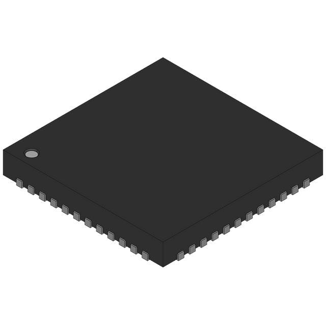
- Part No.:
- DS90C185SQX/NOPB
- Manufacturer:
- Texas Instruments
- Category:
- Serializers, Deserializers
- Package:
- -
- Datasheet:
-
 DS90C185SQX/NOPB.pdf
- Description:
- DS90C185 LOW POWER FPD-LINK (LVD
- Quantity:
- Payment:

- Shipping:

Inventory:2,500
Please send an inquiry. Send us your inquiry, and we will respond immediately.
Product details
Overview
DS90C185SQX/NOPB from Texas Instruments is a low-power 1.8V LVDS serializer for portable display interfaces, converting 28-bit LVCMOS video (24-bit RGB + HSync/VSynch/DE + GPO) into FPD-Link 4D+C LVDS output. It supports SXGA+ (1400×1050@60Hz), operates from 25–105 MHz pixel clock, delivers 2.94 Gbps max throughput, and features sleep mode, spread-spectrum clock compatibility, and VOD-selectable LVDS drivers. It is used in media tablets and netbooks to replace bulky parallel RGB traces with compact differential pairs.
For engineers reviewing the DS90C185SQX/NOPB datasheet, DS90C185SQX/NOPB pinout, DS90C185SQX/NOPB application, or DS90C185SQX/NOPB equivalent, key selection criteria include 24/18-bit RGB mode configurability, 1.8V single-supply operation, WQFN-48 thermal performance, LVDS output compliance per ANSI/TIA/EIA-644–A, and power-down behavior under PDB control.
Technical Context
The DS90C185SQX/NOPB implements a parallel-to-LVDS serialization pipeline with integrated PLL, accepting 28 LVCMOS inputs at up to 105 MHz and generating four LVDS data lanes plus one LVDS clock lane (4D+C). Its internal architecture includes edge-selectable latching (via RFB pin), programmable VOD (±180 mV or ±300 mV), and tri-state control of TxOUT3 in 18-bit mode.
It supports two deterministic operating modes: 24-bit RGB (4D+C, all four TxOUT channels active) and 18-bit RGB (3D+C, TxOUT3 disabled), with independent power management via PDB (sleep mode draws ≤200 µA) and VOD_SEL (reduced swing lowers power by ~20% at 75 MHz). The device requires no external reference clock and locks to the incoming pixel clock.
Key Specifications
| Parameter | Value and Actual Design Meaning |
|---|---|
| Supply Voltage | 1.71–1.89 V - Single 1.8V rail powers core, I/O, and LVDS drivers; eliminates need for multiple supplies. |
| Pixel Clock Range | 25–105 MHz - Enables support from VGA to SXGA+ resolution at 60 Hz with precise timing alignment. |
| Max Throughput | 2.94 Gbps - Achieved at 105 MHz × 28 bits; sufficient for 24-bit RGB @ 1400×1050@60Hz. |
| LVDS Output VOD | ±180 mV (low-power) or ±300 mV (long-cable) - Configurable via VOD_SEL pin; meets ANSI/TIA/EIA-644–A. |
| Power Dissipation | 50 mW typical at 75 MHz - Enabled by full LVCMOS design and 1.8V operation; critical for battery-powered devices. |
| Operating Temp | −10°C to +70°C - Qualified for commercial portable display applications including netbooks and e-readers. |
| Sleep Current | ≤200 µA - Achieved when PDB = 0; shuts down PLL and LVDS drivers while preserving configuration state. |
Pinout & Package
The DS90C185SQX/NOPB is housed in a thermally enhanced 6 mm × 6 mm × 0.8 mm WQFN-48 package with exposed thermal pad (DAP = GND). Pin pitch is 0.5 mm; RoHS-compliant, green (halogen-free) finish; MSL Level-1.
| Pin/Terminal | Circuit Role | Design Meaning |
|---|---|---|
| D0–D27 | LVCMOS Video Input | 28-bit parallel bus: 8R/8G/8B + HSync/VSynch/DE + GP bit; all 1.8V-tolerant with internal pull-downs. |
| CLK | LVCMOS Pixel Clock Input | Primary timing reference; latches input data on rising or falling edge per RFB pin setting. |
| TxOUT0± to TxOUT3± | LVDS Data Outputs | Four differential data lanes; TxOUT3± tri-stated in 18-bit mode to reduce power and EMI. |
| TxCLKOUT± | LVDS Clock Output | Differential clock synchronized to serialized data; 100 Ω DC-coupled load required. |
| PDB | Active-High Sleep Control | Drives device into ultra-low-power state (<200 µA); default = LOW (sleep on power-up). |
| 18B_MODE | Color Depth Select | LOW = 24-bit RGB (4D+C); HIGH = 18-bit RGB (3D+C); overrides VOD_SEL in sleep mode. |
| VOD_SEL | VOD Configuration | LOW = ±180 mV (lower power); HIGH = ±300 mV (longer trace/cable drive); default = HIGH. |
| RFB | Input Edge Select | LOW = latch on falling CLK edge; HIGH = latch on rising edge; enables timing flexibility with receiver. |
Key Features
| Feature | Design Value |
|---|---|
| Single 1.8V Supply Operation | Eliminates dual-rail design complexity and reduces BOM count; simplifies power sequencing and filtering. |
| Configurable 24-/18-bit RGB Mode | Reduces LVDS channel count and power by 25% in 18-bit mode; maintains compatibility with legacy TCONs. |
| Programmable LVDS Output Swing | Enables system-level trade-off between signal integrity (±300 mV) and power efficiency (±180 mV). |
| Integrated Sleep Mode (PDB) | Reduces standby current to ≤200 µA; essential for display blacking and rapid panel power cycling. |
| Spread Spectrum Clock Compatibility | Supports jitter-reduction techniques without requiring external clock synthesis; improves EMI compliance. |
Applications
| eBook Display Interface | Media Tablet Video Link |
|---|---|
Use Scenario: High-resolution grayscale or color eInk/LCD panel driven by ARM-based SoC with limited PCB real estate. IC Role / Device Role / Timing Role: Serializer translating SoC's parallel RGB interface to compact 4D+C LVDS for low-noise, EMI-resistant panel connection. Use Value: Reduces interconnect width from 30+ single-ended traces to 10 differential pairs; enables thinner bezels and longer flex cable routing. | Use Scenario: 10.1-inch IPS LCD module in Android tablet with GPU-driven video pipeline and dynamic backlight control. IC Role / Device Role / Timing Role: Timing-critical serializer synchronizing GPU pixel clock to panel timing controller (TCON) via LVDS physical layer. Use Value: Supports 1400×1050@60Hz with <2.5 ns hold time margin; allows seamless transition between active video and black-frame sleep states. |
| Netbook Main Display Driver | Portable Medical Monitor Interface |
Use Scenario: Integrated graphics output in Intel Atom-based netbook connecting to 1366×768 or 1400×1050 LCD panel. IC Role / Device Role / Timing Role: Bridge IC converting LVCMOS video bus to FPD-Link-compatible LVDS; handles DE/HS/VS signaling and L/R stereo control. Use Value: Enables use of standard LVDS panels without custom TCON firmware; supports 18-bit mode for lower power during idle UI rendering. | Use Scenario: Compact diagnostic monitor in portable ultrasound or patient vital sign equipment requiring reliable, low-jitter video transmission. IC Role / Device Role / Timing Role: Robust serializer with ±300 mV VOD and cycle-to-cycle jitter <0.035 UI at 105 MHz for artifact-free imaging. Use Value: Meets medical EMC requirements via spread-spectrum support and tightly controlled LVDS edge rates (0.18–0.5 ns). |
Equivalent & Alternatives
The following parts are listed as comparable options for similar LVDS serializer applications.
| Alternative Part | Technical Difference | Application Difference | Selection Advice |
|---|---|---|---|
| DS90C187SQX/NOPB | Pin-compatible upgrade with identical pinout, same 48-pin WQFN package, and extended 125 MHz pixel clock support. | Supports UXGA (1600×1200@60Hz); adds enhanced spread-spectrum modulation and improved jitter specs. | Select DS90C187SQX/NOPB for future-proofing high-resolution displays or tighter timing budgets. |
| SN65LVDS93IPWPR | 28-bit LVDS serializer in TSSOP-48; operates from 3.3V supply; lacks VOD_SEL, 18B_MODE, and spread-spectrum support. | Targeted at industrial panels with fixed 3.3V infrastructure; higher power (120 mW typ) and no sleep mode. | Choose SN65LVDS93IPWPR only if 3.3V supply is mandatory and power/performance trade-offs are acceptable. |
Compared with DS90C187SQX/NOPB, DS90C185SQX/NOPB offers lower cost and proven qualification for portable battery life but limits max resolution to SXGA+. Versus SN65LVDS93IPWPR, it provides superior power efficiency, flexible voltage operation, and advanced power management-critical for mobile designs.
Availability
DS90C185SQX/NOPB is available at Aetrix Electronics and suitable for media tablets, netbooks, and portable medical monitors requiring stable component supply, long-term lifecycle assurance, and RoHS-compliant packaging.
Supply support for DS90C185SQX/NOPB includes scheduled delivery planning, volume procurement assistance, BOM continuity management, traceable sourcing, and lifecycle availability coordination for OEM customers, industrial embedded developers, connected-device designers, and electronics production programs.
Manufacturer
Texas Instruments is a global semiconductor leader specializing in analog, embedded processing, and connectivity technologies, with decades of expertise in high-speed interface solutions.
The DS90C185SQX/NOPB belongs to TI's FPD-Link serializer family, engineered specifically for low-power, high-resolution display interfaces in portable consumer and industrial electronics.
FAQ
What is the maximum supported resolution and refresh rate for DS90C185SQX/NOPB?
The DS90C185SQX/NOPB supports up to SXGA+ resolution (1400×1050) at 60 Hz with 24-bit color depth. This is achieved using its full 28-bit LVCMOS input bus (24 RGB + 3 control + 1 GP) and 4D+C LVDS output at 105 MHz pixel clock, delivering 2.94 Gbps total throughput. Lower resolutions such as WXGA or XGA are also fully supported across the 25–105 MHz clock range.
Does DS90C185SQX/NOPB require an external reference clock?
No, DS90C185SQX/NOPB does not require an external reference clock. It uses the incoming LVCMOS pixel clock (CLK) as both timing reference and PLL input. The internal PLL locks directly to this clock, eliminating the need for crystal oscillators or clock generators. This simplifies layout and reduces BOM cost while maintaining tight skew control across LVDS outputs.
How does the PDB pin affect DS90C185SQX/NOPB operation?
The PDB (Power Down Bar) pin is an active-high control that places DS90C185SQX/NOPB into ultra-low-power sleep mode when driven LOW. In sleep mode, the PLL shuts down, LVDS drivers power off and terminate to GND via 100 Ω resistors, and supply current drops to ≤200 µA. The device retains pin configuration state and resumes normal operation within 100 ns after PDB is asserted HIGH.
Can DS90C185SQX/NOPB drive standard LVDS receivers compliant with ANSI/TIA/EIA-644–A?
Yes, DS90C185SQX/NOPB LVDS outputs comply fully with ANSI/TIA/EIA-644–A. Its differential output voltage (VOD) is configurable between ±180 mV and ±300 mV, both within the standard's 250–450 mVpp specification range. Output offset voltage (VOS) is tightly controlled at 0.8–1.0 V, and common-mode noise rejection is ensured by matched rise/fall times (0.18–0.5 ns) and channel-to-channel skew <110 ps.
What is the function of the RFB pin on DS90C185SQX/NOPB?
The RFB (Rising/Falling Edge Bit) pin selects the clock edge used to latch LVCMOS video data. When RFB = LOW (default, pulled down), data is sampled on the falling edge of CLK; when RFB = HIGH, sampling occurs on the rising edge. This allows timing alignment flexibility with the source GPU or TCON, independent of the downstream deserializer's strobe polarity.
DS90C185SQX/NOPB Specifications
- Product attributes
- Attribute value
- Manufacturer:
- Texas Instruments
- Series:
- *
- Package/Case:
- -
- Packaging:
- Bulk
- Product Status:
- Active
- Function:
- -
- Data Rate:
- -
- Input Type:
- -
- Output Type:
- -
- Number of Inputs:
- -
- Number of Outputs:
- -
- Voltage - Supply:
- -
- Operating Temperature:
- -
- Grade:
- -
- Qualification:
- -
- Mounting Type:
- -
- Supplier Device Package:
- -
DS90C185SQX/NOPB FAQ
1.How can I place an order for DS90C185SQX/NOPB through Aetrix?
Please submit a Request for Quotation (RFQ) for DS90C185SQX/NOPB on Aetrix. Our sales agent will provide a competitive quotation and guide you through the order confirmation once you accept the terms.
2.Are the price and stock information for DS90C185SQX/NOPB reliable?
The price and inventory of DS90C185SQX/NOPB are updated periodically and may fluctuate due to market conditions. Stock and pricing data are typically refreshed every 24 hours. Quotation validity for DS90C185SQX/NOPB is usually 5 days.
3.What payment methods are accepted for DS90C185SQX/NOPB?
We accept Wire Transfer, PayPal, Credit Card, Western Union, MoneyGram, and Escrow for DS90C185SQX/NOPB transactions.
Note: Certain payment methods may incur a processing fee.
4.How is shipping managed for DS90C185SQX/NOPB?
DS90C185SQX/NOPB orders can be shipped via leading logistics carriers, including DHL, UPS, FedEx, TNT, or Registered Mail.
Once your DS90C185SQX/NOPB order is processed, you will receive an email with the shipment details and tracking number.
Note: Tracking information may take up to 24 hours to appear. Express delivery typically takes 3–5 business days.
5.How can I obtain technical support or documentation for DS90C185SQX/NOPB?
For technical support, including DS90C185SQX/NOPB datasheets, pinout diagrams, or application guidance, please contact our engineering support team. They can provide detailed documentation and assistance for your DS90C185SQX/NOPB requirements.
6.How does Aetrix verify that DS90C185SQX/NOPB is sourced from the original manufacturer or authorized distributors?
All DS90C185SQX/NOPB products on Aetrix are procured from qualified distributors and authorized channels. Our dedicated quality assurance team conducts strict verification, including traceability checks and, if necessary, third-party testing. This ensures that DS90C185SQX/NOPB meets industry standards.
7.What is the process for return or replacement of DS90C185SQX/NOPB?
All DS90C185SQX/NOPB units undergo pre-shipment inspection (PSI). If there is an issue with DS90C185SQX/NOPB, returns or replacements are accepted under the following conditions:
1.Quantity discrepancies, incorrect items, or visible external defects (such as breakage or corrosion), acknowledged by Aetrix.
2.The issue is reported within 90 days of delivery.
3.The DS90C185SQX/NOPB part is unused and in its original packaging.
Return procedure for DS90C185SQX/NOPB:
1.Submit a request within 90 days.
2.Obtain a Return Material Authorization (RMA) from Aetrix.
DS90C185SQX/NOPB Tags

-
SN65HVS880PWPR
Texas Instruments
-
SN65HVS882PWPR
Texas Instruments

-
FIN3386MTDX
onsemi
-
FIN3385MTDX
onsemi

-
SN65LV1023ARHBR
Texas Instruments

-
SN65LV1023ADBR
Texas Instruments
-
SN65LV1224BDBR
Texas Instruments

-
SN65LVDS93ADGGR
Texas Instruments
-
SN65LVDS93DGGR
Texas Instruments

-
TDES954RGZT
Texas Instruments
-
SN65LV1224BRHBT
Texas Instruments

-
DS90UB914QSQE/NOPB
Texas Instruments
Tech Hub

A practical engineering guide to 3.3V and 5V logic compatibility, input thresholds, resistor dividers, translator ICs, MOSFET level shifting, I2C pull-ups, timing limits and power-sequencing risks.

The 74HC595 uses push-pull logic outputs, while the TPIC6B595 uses 50 V open-drain DMOS sinks for higher-power loads. This guide compares timing, current limits, 3.3 V interfacing, load wiring, thermal…

The 74HC595 converts serial data into eight stable parallel outputs. This guide covers pin functions, shift and storage timing, OE and MR behavior, drive-current limits, cascading, voltage compatibilit…

A technical comparison of level-sensitive latches and edge-triggered flip-flops, covering timing windows, setup and hold limits, master–slave operation, time borrowing, race-through, HDL inference and…

A D latch stores one bit while Enable controls when data can pass. This reference covers gate-level operation, truth tables, transparency, setup and hold timing, LE versus OE, common ICs and practical …

An SR latch stores one bit through cross-coupled feedback. This engineering reference covers NOR and NAND implementations, truth tables, forbidden-state recovery, gated operation, switch debouncing, fa…

Latch circuits retain one bit through feedback. This technical reference covers SR and D latches, truth tables, transparency, timing limits, latch-versus-flip-flop behavior, applications and common log…

An engineering guide to LED driver operation, constant-current and constant-voltage outputs, linear and switching topologies, dimming, IC selection, calculations, replacement compatibility, and fault c…

Operational amplifier guide covering op amp basics, feedback, ideal vs real op amps, common configurations, buffer circuits, offset, bias current, gain-bandwidth, slew rate, rail-to-rail limits and sel…

Jumper cables guide covering safe connection order, red and black clamp placement, final ground connection, cable gauge, length, clamp quality, copper vs CCA cables, jump starter comparison and battery…


