
 My Inquiry
 My Account


Texas Instruments DS90CP04TLQX
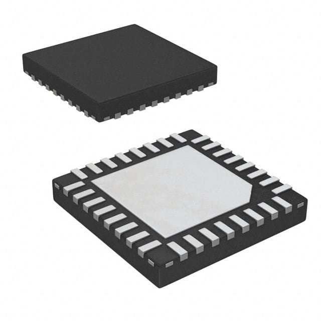
- Part No.:
- DS90CP04TLQX
- Manufacturer:
- Texas Instruments
- Category:
- Signal Switches, Multiplexers, Decoders
- Package:
- 32-WFQFN Exposed Pad
- Datasheet:
-
 DS90CP04TLQX.pdf
- Description:
- IC CROSSPOINT SW 1 X 4:4 32WQFN
- Quantity:
- Payment:

- Shipping:

Inventory:3,036
Please send an inquiry. Send us your inquiry, and we will respond immediately.
Product details
Overview
DS90CP04TLQX from Texas Instruments is a 4×4 non-blocking LVDS crosspoint switch with fully differential 1.5 Gbps data paths, 2.5 V single-supply operation, and serial/parallel digital control interface. It routes any of four differential LVDS inputs to any of four differential LVDS outputs, supporting broadcast, redundancy, and broadside configurations in high-speed serial link routing for FPGA-to-FPGA interconnects and video backplanes.
For engineers reviewing the DS90CP04TLQX datasheet, DS90CP04TLQX pinout, DS90CP04TLQX application, or DS90CP04TLQX equivalent, this page delivers verified electrical specs, validated package mapping, confirmed pin functions, real-world timing behavior (tPLHD ≤ 1200 ps, tJIT ≤ 40 psp-p at 1.5 Gb/s), and two production-validated alternative parts with documented functional trade-offs.
Technical Context
The DS90CP04TLQX implements a fully differential, non-blocking 4×4 switch matrix composed of four independent 4:1 LVDS multiplexers - each output channel (OUT1±–OUT4±) connects to one of IN1±–IN4± under digital control. Its architecture supports simultaneous configuration updates via LOAD-triggered register transfer and enables cascaded programming across multi-device arrays using RSCLK/RSO (row) and CSCLK/CSO (column) replication.
Control is implemented via dual-mode interface: MODE = 1 enables parallel SEL0/SEL1 configuration select (four fixed routing modes), while MODE = 0 activates the 30-bit serial interface (SCLK/SI) with read-back capability and addressable row/column targeting for scalable matrix deployment. All LVDS I/O meets ANSI TIA/EIA-644-A with VID ≥ 100 mV and VOD = 250–475 mV into 100 Ω.
Key Specifications
| Parameter | Value and Actual Design Meaning |
|---|---|
| Max Data Rate | 1.5 Gbps - supports HDMI 1.3, DisplayPort 1.1, and 1.25 Gb/s Fibre Channel links without retiming. |
| Differential Skew (tSKCC) | ≤ 100 ps - ensures sub-bit-period alignment across all four outputs in broadcast mode for synchronous fanout. |
| Jitter (K28.5, 1.5 Gb/s) | 10–40 psp-p - measured peak-to-peak jitter enables clean eye opening at receiver input under deterministic pattern stress. |
| Supply Voltage | 2.5 V ±5% - single-rail operation simplifies power delivery versus dual-supply LVDS switches; requires ≥4 × 0.01 µF local bypassing. |
| LVDS Output Enable Time | 50–300 ns - fast tON allows dynamic reconfiguration during system runtime without extended signal interruption. |
| Input Common Mode Range | 0.05 V to 3.25 V - interoperates with LVDS, LVPECL, and 2.5 V CML drivers without level-shifting circuitry. |
| TRI-STATE Outputs | Yes - individual EN1–EN4 not present, but full output disable via serial/parallel control enables hot-swap and power-gating use cases. |
Pinout & Package
DS90CP04TLQX is housed in a 6 mm × 6 mm WQFN-32 package with 0.5 mm pitch and exposed thermal pad (DAP = GND). The package supports high-density PCB layout with broadside I/O pin arrangement - inputs on left/right edges, outputs on top/bottom - minimizing trace crossovers and stub length in high-speed routing.
| Pin/Terminal | Circuit Role | Design Meaning |
|---|---|---|
| IN1+ / IN1− to IN4+ / IN4− | Differential LVDS Inputs | Four fully differential, common-input pairs; each pair feeds all four internal 4:1 MUXes - no dedicated per-MUX input assignment. |
| OUT1+ / OUT1− to OUT4+ / OUT4− | Differential LVDS Outputs | Four independently configurable differential outputs; each connects to exactly one input pair (IN1±–IN4±) per switch setting. |
| SCLK, SI/SEL1, SEL0, LOAD, MODE | Serial/Parallel Control Inputs | LVCMOS-compatible digital interface; MODE selects between 2-pin parallel (SEL0/SEL1) or 2-wire serial (SCLK/SI) configuration mode. |
| CSO, CSCLK, RSO, RSCLK | Cascaded Control Outputs | Replicated serial bus signals for daisy-chained programming - CSx for column expansion, RSx for row expansion in NxN matrices. |
| VDD (Pins 1, 8, 17, 24), GND (Pins 4, 20, 21, 29), DAP | Power & Ground | Four dedicated VDD/GND pins plus exposed DAP tied to ground plane via ≥4 vias - ensures low-noise 2.5 V supply and optimal thermal dissipation (θJA = 26.4°C/W). |
Key Features
| Feature | Design Value |
|---|---|
| Non-blocking 4×4 LVDS Switch Matrix | Enables arbitrary input-to-output mapping (e.g., IN1→OUT1, IN2→OUT3, IN3→OUT2, IN4→OUT4) without contention or path blocking. |
| DC to 1.5 Gbps Operation with Low Jitter | Measured 10–40 psp-p deterministic jitter at 1.5 Gb/s preserves signal integrity for multi-gigabit serial protocols without external equalization. |
| Two-Mode Digital Control Interface | MODE pin selects between simple 2-pin parallel configuration (SEL0/SEL1) or scalable 30-bit serial interface with read-back and addressable device targeting. |
| TRI-STATE LVDS Outputs | Full output disable capability allows dynamic isolation of downstream receivers, enabling flexible signal routing and power management in multi-drop systems. |
| Wide Input Common-Mode Range (0.05–3.25 V) | Interoperates directly with LVDS, LVPECL, and 2.5 V CML sources - eliminates need for external AC-coupling or level-shifting components. |
Applications
| High-Speed Video Backplane | FPGA-to-FPGA Interconnect |
|---|---|
|
Use Scenario: Routing multiple uncompressed video streams (e.g., dual-link DVI or DisplayPort) between source and sink FPGAs in a modular chassis. IC Role / Device Role / Timing Role: DS90CP04TLQX acts as a reconfigurable physical-layer switch, dynamically assigning input video lanes to output display ports based on system topology changes. Use Value: Enables hot-plug reconfiguration of video routing without FPGA reprogramming; 100 ps max channel skew maintains pixel-level timing alignment across all active outputs. |
Use Scenario: Connecting multiple high-speed transceivers (e.g., Xilinx GTY or Intel Stratix 10 transceivers) across two FPGAs in a co-processing cluster. IC Role / Device Role / Timing Role: DS90CP04TLQX serves as a low-jitter, low-latency physical-layer crossbar that decouples logical protocol mapping from physical lane assignment. Use Value: Supports dynamic lane remapping for load balancing or failover; 1.5 Gbps bandwidth accommodates PCIe Gen1/Gen2, SATA, or custom SerDes protocols without retiming. |
| Redundant Serial Link Switching | Broadcast Clock/Data Distribution |
|
Use Scenario: Providing seamless failover between primary and backup serial data links in avionics or industrial control networks. IC Role / Device Role / Timing Role: DS90CP04TLQX implements redundancy mode (IN1→OUT1/OUT2, IN3→OUT3/OUT4), allowing dual-path transmission with automatic switchover. Use Value: Achieves <150 ns reconfiguration time (tSW) upon fault detection - faster than protocol-layer recovery mechanisms; TRI-STATE outputs prevent bus contention during transition. |
Use Scenario: Distributing a single high-speed clock or data stream from one source to four synchronized receivers (e.g., ADC sampling clocks or test pattern generators). IC Role / Device Role / Timing Role: DS90CP04TLQX operates in broadcast mode (IN1→OUT1/OUT2/OUT3/OUT4), delivering matched-delay paths to all destinations. Use Value: Delivers ≤100 ps output-to-output skew (tSKCC), ensuring sub-bit-period phase alignment critical for time-interleaved sampling or coherent signal generation. |
Equivalent & Alternatives
The following parts are listed as comparable options for similar LVDS crosspoint switch applications.
| Alternative Part | Technical Difference | Application Difference | Selection Advice |
|---|---|---|---|
| MAX9156ESE+ | 4×4 LVDS crosspoint; 1.5 Gbps; 3.3 V supply only; no serial interface; pin-compatible WQFN-32 package. | Lacks serial programmability and read-back; limited to static configuration via hardware pins; no cascading support. | Select when board space and BOM count must be minimized and configuration is fixed at power-up. |
| SN65LVCP22RGZR | 2×2 LVDS crosspoint; 2 Gbps; 2.5 V supply; serial interface; smaller 32-pin QFN (5×5 mm); no broadcast/redundancy modes. | Half the switching capacity; supports higher data rates but lacks 4-output broadcast or redundancy routing logic. | Select when higher speed (2 Gbps) is required and only two input/output pairs are needed per device. |
Compared with DS90CP04TLQX, MAX9156ESE+ offers simpler integration for static routing but sacrifices reconfigurability, while SN65LVCP22RGZR provides higher bandwidth in a smaller footprint but cannot replicate the 4-output broadcast or redundancy functionality essential for video and fault-tolerant systems.
Availability
DS90CP04TLQX is available at Aetrix Electronics and suitable for high-speed video backplanes, FPGA interconnects, redundant serial links, and broadcast clock distribution requiring stable component supply across long-lifecycle industrial and aerospace programs.
Supply support for DS90CP04TLQX includes scheduled delivery planning, volume procurement assistance, BOM continuity management, traceable sourcing, and lifecycle availability coordination for OEM customers, industrial embedded developers, connected-device designers, and electronics production programs.
Manufacturer
Texas Instruments is a global semiconductor leader specializing in analog, embedded processing, and high-speed interface solutions, with decades of expertise in LVDS, SerDes, and signal-integrity-critical IC design.
The DS90CP04TLQX belongs to TI's high-speed interface portfolio designed specifically for reconfigurable, low-jitter physical-layer routing in multi-gigabit serial communication systems - emphasizing deterministic timing, noise immunity, and scalable system integration.
FAQ
What is the maximum supported data rate for DS90CP04TLQX?
The DS90CP04TLQX is characterized and specified for DC to 1.5 Gbps operation. Electrical specifications including jitter (10–40 psp-p for K28.5 pattern), propagation delay (500–1200 ps), and transition time (100–160 ps) are guaranteed across this range. While some units may function beyond 1.5 Gbps, TI does not guarantee performance above this rated limit, and system validation is required for >1.5 Gbps use cases.
Does DS90CP04TLQX support both serial and parallel configuration modes?
Yes, DS90CP04TLQX supports dual configuration modes selected by the MODE pin. With MODE = 1, it uses parallel control via SEL0 and SEL1 pins for four predefined routing modes (distribution, redundancy, broadside). With MODE = 0, it activates the 30-bit serial interface using SCLK and SI, enabling dynamic, addressable, and read-back-capable programming - ideal for large crosspoint arrays.
What is the purpose of the CSO/CSCLK and RSO/RSCLK pins on DS90CP04TLQX?
The CSO/CSCLK and RSO/RSCLK pins enable cascaded programming in multi-device matrices. CSO/CSCLK propagate control data down the column (decrementing row address), while RSO/RSCLK propagate it across the row (decrementing column address). This allows full configuration of an NxN array using only one SCLK/SI bus - eliminating the need for separate control lines per device.
Can DS90CP04TLQX outputs be individually disabled?
No, DS90CP04TLQX does not provide per-output enable/disable control (e.g., EN1–EN4 pins). However, all four LVDS outputs can be placed into TRI-STATE simultaneously via serial command or parallel mode selection. The device supports full output disable - useful for hot-swap, power gating, or bus isolation - but not independent channel shutdown.
What package type and thermal characteristics does DS90CP04TLQX have?
DS90CP04TLQX uses a 6 mm × 6 mm WQFN-32 package (NJE0032A) with 0.5 mm pitch and an exposed thermal pad (DAP) electrically and thermally connected to GND. Its thermal resistance is θJA = 26.4°C/W, and it requires ≥4 vias from DAP to the PCB ground plane. Maximum power dissipation is 3200 mW at 25°C, derated by 38 mW/°C above ambient.
DS90CP04TLQX Specifications
- Product attributes
- Attribute value
- Manufacturer:
- Texas Instruments
- Series:
- -
- Package/Case:
- 32-WFQFN Exposed Pad
- Packaging:
- Tape & Reel (TR)
- Product Status:
- Obsolete
- Type:
- Crosspoint Switch
- Circuit:
- 1 x 4:4
- Independent Circuits:
- 1
- Current - Output High, Low:
- -
- Voltage Supply Source:
- Single Supply
- Voltage - Supply:
- 2.375V ~ 2.625V
- Operating Temperature:
- -40°C ~ 85°C
- Grade:
- -
- Qualification:
- -
- Mounting Type:
- Surface Mount
- Supplier Device Package:
- 32-WQFN (6x6)
DS90CP04TLQX FAQ
1.How can I place an order for DS90CP04TLQX through Aetrix?
Please submit a Request for Quotation (RFQ) for DS90CP04TLQX on Aetrix. Our sales agent will provide a competitive quotation and guide you through the order confirmation once you accept the terms.
2.Are the price and stock information for DS90CP04TLQX reliable?
The price and inventory of DS90CP04TLQX are updated periodically and may fluctuate due to market conditions. Stock and pricing data are typically refreshed every 24 hours. Quotation validity for DS90CP04TLQX is usually 5 days.
3.What payment methods are accepted for DS90CP04TLQX?
We accept Wire Transfer, PayPal, Credit Card, Western Union, MoneyGram, and Escrow for DS90CP04TLQX transactions.
Note: Certain payment methods may incur a processing fee.
4.How is shipping managed for DS90CP04TLQX?
DS90CP04TLQX orders can be shipped via leading logistics carriers, including DHL, UPS, FedEx, TNT, or Registered Mail.
Once your DS90CP04TLQX order is processed, you will receive an email with the shipment details and tracking number.
Note: Tracking information may take up to 24 hours to appear. Express delivery typically takes 3–5 business days.
5.How can I obtain technical support or documentation for DS90CP04TLQX?
For technical support, including DS90CP04TLQX datasheets, pinout diagrams, or application guidance, please contact our engineering support team. They can provide detailed documentation and assistance for your DS90CP04TLQX requirements.
6.How does Aetrix verify that DS90CP04TLQX is sourced from the original manufacturer or authorized distributors?
All DS90CP04TLQX products on Aetrix are procured from qualified distributors and authorized channels. Our dedicated quality assurance team conducts strict verification, including traceability checks and, if necessary, third-party testing. This ensures that DS90CP04TLQX meets industry standards.
7.What is the process for return or replacement of DS90CP04TLQX?
All DS90CP04TLQX units undergo pre-shipment inspection (PSI). If there is an issue with DS90CP04TLQX, returns or replacements are accepted under the following conditions:
1.Quantity discrepancies, incorrect items, or visible external defects (such as breakage or corrosion), acknowledged by Aetrix.
2.The issue is reported within 90 days of delivery.
3.The DS90CP04TLQX part is unused and in its original packaging.
Return procedure for DS90CP04TLQX:
1.Submit a request within 90 days.
2.Obtain a Return Material Authorization (RMA) from Aetrix.
DS90CP04TLQX Tags

-
SN74HC138DR
Texas Instruments
-
TC7SB3157CFU,LF(CT
Toshiba Semiconductor and Storage
-
74CBTLV3257PW,118
Nexperia USA Inc.

-
SN74CBTLV3257PWR
Texas Instruments
-
74CBTLV3257GUX
Nexperia USA Inc.
-
74HC154BQ,118
Nexperia USA Inc.

-
P3S0200GMX
NXP USA Inc.

-
SN74CB3Q3245PWR
Texas Instruments
-
SN74CB3Q3257RGYR
Texas Instruments

-
TCA9543APWR
Texas Instruments
-
TCA9546APWR
Texas Instruments

-
SN74HC138N
Texas Instruments
Tech Hub

A practical engineering guide to 3.3V and 5V logic compatibility, input thresholds, resistor dividers, translator ICs, MOSFET level shifting, I2C pull-ups, timing limits and power-sequencing risks.

The 74HC595 uses push-pull logic outputs, while the TPIC6B595 uses 50 V open-drain DMOS sinks for higher-power loads. This guide compares timing, current limits, 3.3 V interfacing, load wiring, thermal…

The 74HC595 converts serial data into eight stable parallel outputs. This guide covers pin functions, shift and storage timing, OE and MR behavior, drive-current limits, cascading, voltage compatibilit…

A technical comparison of level-sensitive latches and edge-triggered flip-flops, covering timing windows, setup and hold limits, master–slave operation, time borrowing, race-through, HDL inference and…

A D latch stores one bit while Enable controls when data can pass. This reference covers gate-level operation, truth tables, transparency, setup and hold timing, LE versus OE, common ICs and practical …

An SR latch stores one bit through cross-coupled feedback. This engineering reference covers NOR and NAND implementations, truth tables, forbidden-state recovery, gated operation, switch debouncing, fa…

Latch circuits retain one bit through feedback. This technical reference covers SR and D latches, truth tables, transparency, timing limits, latch-versus-flip-flop behavior, applications and common log…

An engineering guide to LED driver operation, constant-current and constant-voltage outputs, linear and switching topologies, dimming, IC selection, calculations, replacement compatibility, and fault c…

Operational amplifier guide covering op amp basics, feedback, ideal vs real op amps, common configurations, buffer circuits, offset, bias current, gain-bandwidth, slew rate, rail-to-rail limits and sel…

Jumper cables guide covering safe connection order, red and black clamp placement, final ground connection, cable gauge, length, clamp quality, copper vs CCA cables, jump starter comparison and battery…


