
 My Inquiry
 My Account


Texas Instruments DS90CR216AMTD-TI
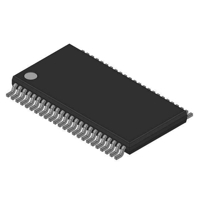
- Part No.:
- DS90CR216AMTD-TI
- Manufacturer:
- Texas Instruments
- Category:
- Specialized
- Package:
- -
- Datasheet:
-
 DS90CR216AMTD-TI.pdf
- Description:
- LINE RECEIVER, 3 FUNC, 3 RCVR, C
- Quantity:
- Payment:

- Shipping:

Inventory:3,704
Please send an inquiry. Send us your inquiry, and we will respond immediately.
Product details
Overview
DS90CR216AMTD-TI from Texas Instruments (formerly National Semiconductor) is a 21-bit Channel Link LVDS receiver IC that converts three LVDS data streams into parallel CMOS/TTL outputs with rising-edge strobe timing. It operates at up to 66 MHz, supports 173 MB/s bandwidth, features 48-lead TSSOP packaging, and delivers <90 mA worst-case supply current at 66 MHz over −40°C to +85°C.
For engineers reviewing the DS90CR216AMTD-TI datasheet, DS90CR216AMTD-TI pinout, DS90CR216AMTD-TI application, or DS90CR216AMTD-TI equivalent, this device is selected for high-speed serial-to-parallel conversion in display interface, industrial camera, and embedded vision systems where EMI reduction and cable size minimization are critical design constraints.
Technical Context
The DS90CR216AMTD-TI implements a dedicated LVDS receiver front-end with integrated PLL and TTL-level clock/data output stage. Its input accepts three differential LVDS data pairs plus one differential LVDS clock pair, all compliant with TIA/EIA-644. The internal PLL requires no external components and locks to incoming clock frequencies between 20 MHz and 66 MHz.
Output timing is synchronized to a rising-edge strobe on RxCLK OUT, with guaranteed setup/hold windows (RSRC/RHRC) as low as 4.5 ns / 4.0 ns at 66 MHz. Skew margin (RSKM) is specified at 400 ps at 66 MHz, enabling robust operation across interconnects with cable skew and jitter up to 250 ps.
Key Specifications
| Parameter | Value and Actual Design Meaning |
|---|---|
| Interface Type | LVDS receiver with TTL/CMOS parallel output - enables high-noise-margin serial link termination for display/camera interfaces |
| Data Width | 21-bit parallel output - matches native pixel bus widths in WVGA and SVGA display controllers |
| Max Data Rate | 1.386 Gbps aggregate throughput - supports 66 MHz × 21 bits with full Channel Link protocol compatibility |
| Supply Voltage | 3.0 V to 3.6 V (typ. 3.3 V) - compatible with standard +3.3V logic rails and LDO-regulated systems |
| Power Consumption | <90 mA worst-case @66 MHz - enables thermal management in dense PCB layouts without forced air |
| Operating Temp | −40°C to +85°C - qualified for industrial and automotive-grade applications per AEC-Q100 Grade 3 |
| ESD Rating | >7 kV HBM - provides robust handling during assembly and field service without additional protection circuitry |
Pinout & Package
DS90CR216AMTD-TI uses a 48-lead TSSOP package (NS MTD48), 7.0 mm × 12.5 mm body, 0.5 mm lead pitch, with exposed thermal pad (not electrically connected). Pin assignments are validated per official National Semiconductor datasheet revision April 2011.
| Pin/Terminal | Circuit Role | Design Meaning |
|---|---|---|
| RxIN+, RxIN− | LVDS differential data inputs (3 pairs) | Accept serialized video/data streams; internal failsafe bias ensures defined state when floating or terminated |
| RxCLK IN+, RxCLK IN− | LVDS differential clock input | Provides reference for PLL lock and output strobe generation; determines maximum operating frequency |
| RxCLK OUT | TTL-level clock output | Rising edge serves as synchronous data strobe for latching 21-bit parallel outputs |
| RxOUT[0:20] | CMOS/TTL parallel data outputs | 21-bit wide bus aligned to RxCLK OUT rising edge; drive standard 50 Ω terminated loads |
| PWR DOWN | Active-low power-down control | Asserting low disables outputs (driven low), reduces supply current to ≤55 μA, and halts PLL operation |
| VCC, GND, PLL VCC, PLL GND, LVDS VCC, LVDS GND | Separate supply/ground domains | Isolates noise-sensitive PLL and LVDS receiver sections from TTL output switching transients |
Key Features
| Feature | Design Value |
|---|---|
| 20–66 MHz shift clock support | Enables flexible timing alignment across variable-resolution display panels and camera sensors |
| 50% duty cycle on RxCLK OUT | Ensures symmetrical timing margins for both setup and hold validation in downstream logic |
| Best-in-class set/hold times (4.5 ns / 4.0 ns @66 MHz) | Reduces timing closure risk in FPGA or ASIC capture logic without added delay compensation |
| Integrated PLL with no external components | Eliminates BOM cost and layout area for loop filter capacitors and resistors |
| Low-power down mode (<55 μA) | Supports dynamic power gating in battery-powered or thermally constrained vision modules |
Applications
| Industrial Camera Interface | Automotive Display Link |
|---|---|
Use Scenario: High-speed image sensor output transmission over coaxial or twisted-pair cable to host processor. IC Role / Device Role / Timing Role: LVDS deserializer converting 3-lane serialized pixel data into 21-bit parallel bus synchronized to rising-edge strobe. Use Value: Enables 66 MHz pixel clock transmission with 400 ps skew margin, reducing EMI and replacing 21+ single-ended traces. | Use Scenario: Driving TFT-LCD panels in automotive instrument clusters or infotainment displays. IC Role / Device Role / Timing Role: Receives serialized video from graphics SoC and reconstructs parallel RGB data with precise strobe-aligned timing. Use Value: Supports AEC-Q100 Grade 3 qualification and −40°C to +85°C operation for under-hood and dashboard environments. |
| Medical Imaging Module | Machine Vision Controller |
Use Scenario: Transmitting real-time ultrasound or endoscope video from probe head to processing unit via compact cabling. IC Role / Device Role / Timing Role: Deserializes LVDS-encoded video frames and outputs TTL-level parallel data with deterministic latency. Use Value: Achieves 173 MB/s bandwidth within 48-pin TSSOP footprint, minimizing connector count and board space in portable devices. | Use Scenario: Interfacing high-resolution line-scan cameras with FPGA-based frame grabbers in factory automation. IC Role / Device Role / Timing Role: Converts serialized sensor data into parallel format with sub-nanosecond strobe positioning accuracy (RSPos0 = 0.7–1.4 ns @66 MHz). Use Value: Guarantees reliable sampling of fast-moving objects by maintaining tight setup/hold windows across temperature and voltage variation. |
Equivalent & Alternatives
The following parts are listed as comparable options for similar LVDS deserializer applications.
| Alternative Part | Technical Difference | Application Difference | Selection Advice |
|---|---|---|---|
| DS90CR218MTD | 24-bit Channel Link receiver; same 48-pin TSSOP package; higher bandwidth (200 MB/s); no AEC-Q100 qualification | Targeted at non-automotive high-resolution imaging where extra data lanes are needed | Select DS90CR218MTD only if 24-bit bus width and >66 MHz operation are required; not drop-in compatible due to pin mapping differences |
| SN65LVDS32 | Single-channel LVDS receiver (4-bit); 16-pin SOIC; no PLL; no parallel output bus or strobe generation | Suitable for point-to-point LVDS signal conditioning, not Channel Link deserialization | Choose SN65LVDS32 only for simple LVDS level-shifting; cannot replace DS90CR216AMTD-TI in serial-to-parallel conversion roles |
Compared with DS90CR216AMTD-TI, DS90CR218MTD offers wider data width but lacks automotive qualification, while SN65LVDS32 provides basic LVDS reception without deserialization capability-neither is pin-compatible, and both require redesign of data path and timing architecture.
Availability
DS90CR216AMTD-TI is available at Aetrix Electronics and suitable for industrial camera interfaces, automotive display links, and medical imaging modules requiring stable component supply, long-term lifecycle support, and traceable sourcing.
Supply support for DS90CR216AMTD-TI includes scheduled delivery planning, volume procurement assistance, BOM continuity management, traceable sourcing, and lifecycle availability coordination for OEM customers, industrial embedded developers, connected-device designers, and electronics production programs.
Manufacturer
Texas Instruments acquired National Semiconductor in 2011 and maintains full technical and supply chain responsibility for legacy Channel Link products including DS90CR216AMTD-TI.
This device belongs to TI's high-speed interface portfolio, designed specifically to replace wide parallel buses in display, imaging, and machine vision systems using low-skew, low-EMI LVDS serialization.
FAQ
What is the function of the PWR DOWN pin on DS90CR216AMTD-TI?
The PWR DOWN pin on DS90CR216AMTD-TI is an active-low control input that places the device into ultra-low-power mode when asserted. In this state, all RxOUT pins are driven low, the internal PLL stops, and supply current drops to ≤55 μA. This feature allows dynamic power management in systems where the display or camera interface may be intermittently active, and it is fully specified across the −40°C to +85°C operating range for DS90CR216AMTD-TI.
Does DS90CR216AMTD-TI support 20 MHz input clock frequency?
Yes, DS90CR216AMTD-TI supports input clock frequencies from 20 MHz to 66 MHz, as confirmed in the "Features" section and electrical specifications table. At 20 MHz, the device maintains full functionality including PLL lock, valid RxCLK OUT generation, and correct 21-bit parallel output timing. The minimum clock specification is explicitly stated and tested across temperature and voltage ranges for DS90CR216AMTD-TI.
What package type does DS90CR216AMTD-TI use, and is it RoHS-compliant?
DS90CR216AMTD-TI uses a 48-lead TSSOP package (National Semiconductor package code MTD48), measuring 7.0 mm × 12.5 mm with 0.5 mm lead pitch. While the original 2011 datasheet does not explicitly declare RoHS status, TI's current product change notices confirm that DS90CR216AMTD-TI is manufactured in RoHS-compliant, lead-free form and meets JEDEC J-STD-020 moisture sensitivity level 3 requirements.
How does DS90CR216AMTD-TI handle floating LVDS inputs?
DS90CR216AMTD-TI includes internal failsafe bias circuitry on all LVDS inputs (RxIN+/- and RxCLK IN+/-). When inputs are floating or properly terminated without signal, the receiver outputs default to a HIGH state. If a valid clock is present, all RxOUT bits follow data; if the clock is also floating, outputs retain their last valid state. This behavior is documented in Note 8 of the DS90CR216AMTD-TI datasheet and ensures predictable startup and fault conditions.
What is the maximum allowable LVDS input common-mode voltage range for DS90CR216AMTD-TI?
The maximum allowable LVDS input common-mode voltage range for DS90CR216AMTD-TI is 0 V to 2.4 V, as specified in the "Recommended Operating Conditions" table. This range ensures compatibility with standard LVDS drivers operating at 3.3 V supply, and the receiver maintains full differential sensitivity (±100 mV thresholds) across this entire common-mode span. Exceeding 2.4 V risks violating absolute maximum ratings and may cause latch-up or parametric degradation in DS90CR216AMTD-TI.
DS90CR216AMTD-TI Specifications
- Product attributes
- Attribute value
- Manufacturer:
- Texas Instruments
- Series:
- *
- Package/Case:
- -
- Packaging:
- Bulk
- Product Status:
- Active
- Applications:
- -
- Interface:
- -
- Voltage - Supply:
- -
- Supplier Device Package:
- -
- Grade:
- -
- Qualification:
- -
- Mounting Type:
- -
DS90CR216AMTD-TI FAQ
1.How can I place an order for DS90CR216AMTD-TI through Aetrix?
Please submit a Request for Quotation (RFQ) for DS90CR216AMTD-TI on Aetrix. Our sales agent will provide a competitive quotation and guide you through the order confirmation once you accept the terms.
2.Are the price and stock information for DS90CR216AMTD-TI reliable?
The price and inventory of DS90CR216AMTD-TI are updated periodically and may fluctuate due to market conditions. Stock and pricing data are typically refreshed every 24 hours. Quotation validity for DS90CR216AMTD-TI is usually 5 days.
3.What payment methods are accepted for DS90CR216AMTD-TI?
We accept Wire Transfer, PayPal, Credit Card, Western Union, MoneyGram, and Escrow for DS90CR216AMTD-TI transactions.
Note: Certain payment methods may incur a processing fee.
4.How is shipping managed for DS90CR216AMTD-TI?
DS90CR216AMTD-TI orders can be shipped via leading logistics carriers, including DHL, UPS, FedEx, TNT, or Registered Mail.
Once your DS90CR216AMTD-TI order is processed, you will receive an email with the shipment details and tracking number.
Note: Tracking information may take up to 24 hours to appear. Express delivery typically takes 3–5 business days.
5.How can I obtain technical support or documentation for DS90CR216AMTD-TI?
For technical support, including DS90CR216AMTD-TI datasheets, pinout diagrams, or application guidance, please contact our engineering support team. They can provide detailed documentation and assistance for your DS90CR216AMTD-TI requirements.
6.How does Aetrix verify that DS90CR216AMTD-TI is sourced from the original manufacturer or authorized distributors?
All DS90CR216AMTD-TI products on Aetrix are procured from qualified distributors and authorized channels. Our dedicated quality assurance team conducts strict verification, including traceability checks and, if necessary, third-party testing. This ensures that DS90CR216AMTD-TI meets industry standards.
7.What is the process for return or replacement of DS90CR216AMTD-TI?
All DS90CR216AMTD-TI units undergo pre-shipment inspection (PSI). If there is an issue with DS90CR216AMTD-TI, returns or replacements are accepted under the following conditions:
1.Quantity discrepancies, incorrect items, or visible external defects (such as breakage or corrosion), acknowledged by Aetrix.
2.The issue is reported within 90 days of delivery.
3.The DS90CR216AMTD-TI part is unused and in its original packaging.
Return procedure for DS90CR216AMTD-TI:
1.Submit a request within 90 days.
2.Obtain a Return Material Authorization (RMA) from Aetrix.
DS90CR216AMTD-TI Tags

-
NVT4857UKAZ
NXP Semiconductors

-
TCA8418RTWR
Texas Instruments

-
PCA9546APWR
Texas Instruments

-
MD0100N8-G
Microchip Technology

-
PCA9548APW,118
NXP Semiconductors

-
PCA9540BDP,118
NXP Semiconductors

-
PCA9548APWR
Texas Instruments

-
PCA9546APW,118
NXP Semiconductors

-
PTN3360DBS,518
NXP Semiconductors

-
PCA9546ABS,118
NXP Semiconductors

-
PCA9518PWR
Texas Instruments

-
PCA9545APW,118
NXP Semiconductors
Tech Hub

A practical engineering guide to 3.3V and 5V logic compatibility, input thresholds, resistor dividers, translator ICs, MOSFET level shifting, I2C pull-ups, timing limits and power-sequencing risks.

The 74HC595 uses push-pull logic outputs, while the TPIC6B595 uses 50 V open-drain DMOS sinks for higher-power loads. This guide compares timing, current limits, 3.3 V interfacing, load wiring, thermal…

The 74HC595 converts serial data into eight stable parallel outputs. This guide covers pin functions, shift and storage timing, OE and MR behavior, drive-current limits, cascading, voltage compatibilit…

A technical comparison of level-sensitive latches and edge-triggered flip-flops, covering timing windows, setup and hold limits, master–slave operation, time borrowing, race-through, HDL inference and…

A D latch stores one bit while Enable controls when data can pass. This reference covers gate-level operation, truth tables, transparency, setup and hold timing, LE versus OE, common ICs and practical …

An SR latch stores one bit through cross-coupled feedback. This engineering reference covers NOR and NAND implementations, truth tables, forbidden-state recovery, gated operation, switch debouncing, fa…

Latch circuits retain one bit through feedback. This technical reference covers SR and D latches, truth tables, transparency, timing limits, latch-versus-flip-flop behavior, applications and common log…

An engineering guide to LED driver operation, constant-current and constant-voltage outputs, linear and switching topologies, dimming, IC selection, calculations, replacement compatibility, and fault c…

Operational amplifier guide covering op amp basics, feedback, ideal vs real op amps, common configurations, buffer circuits, offset, bias current, gain-bandwidth, slew rate, rail-to-rail limits and sel…

Jumper cables guide covering safe connection order, red and black clamp placement, final ground connection, cable gauge, length, clamp quality, copper vs CCA cables, jump starter comparison and battery…


