
 My Inquiry
 My Account


Texas Instruments DS90UR910QSQE/NOPB
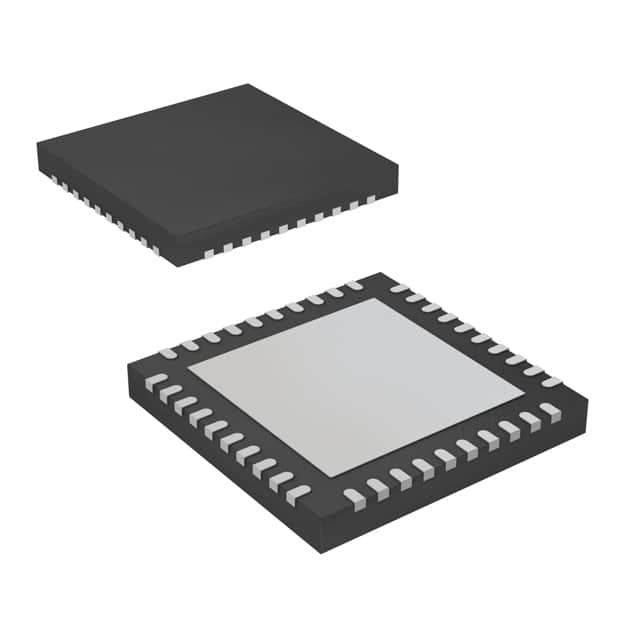
- Part No.:
- DS90UR910QSQE/NOPB
- Manufacturer:
- Texas Instruments
- Category:
- Serializers, Deserializers
- Package:
- 40-WFQFN Exposed Pad
- Datasheet:
-
 DS90UR910QSQE/NOPB.pdf
- Description:
- IC SERIALIZER FPD-CSI2 48WQFN
- Quantity:
- Payment:

- Shipping:

Inventory:2,050
Please send an inquiry. Send us your inquiry, and we will respond immediately.
Product details
Overview
DS90UR910QSQE/NOPB from Texas Instruments is an automotive-grade FPD-Link II to MIPI CSI-2 bridge converter that recovers 24-bit RGB video and sync signals (HS/VS/DE/PCLK) from a single-pair FPD-Link II serial stream and retransmits them as two-lane CSI-2 D-PHY output. It supports pixel clocks from 10 MHz to 75 MHz (280 Mbps–2.1 Gbps linerate), operates on a single 1.8-V supply, and delivers up to 900 Mbps per CSI-2 lane for use in central infotainment displays and digital instrument clusters.
For engineers reviewing the DS90UR910QSQE/NOPB datasheet, DS90UR910QSQE/NOPB pinout, DS90UR910QSQE/NOPB application, or DS90UR910QSQE/NOPB equivalent, this page provides verified technical context, validated pin functions, confirmed AEC-Q100 Grade 2 qualification, exact CSI-2 timing compliance (v1.01), and real-world automotive interface constraints including STP cable reach up to 10 meters and integrated equalization for variable-length interconnects.
Technical Context
The DS90UR910QSQE/NOPB implements a full FPD-Link II deserializer with CML input receiver (RIN±), adaptive receive equalization (EQ[3:1]), fast random-lock PLL (no reference clock required), and MIPI D-PHY v1.00.00-compliant transmitter with dual HS data lanes (DATA0±/DATA1±) and half-rate clock lane (CLK±). It performs packetization of RGB888 video streams into CSI-2 format with continuous/non-continuous clocking support.
It integrates configurable control interfaces (CCI/I²C), BIST with PASS/LOCK status reporting, ultra-low power state (ULPS) entry/exit in 1 ms, and 1.8-V/3.3-V LVCMOS I/O compatibility via VDDIO. All analog, digital, and CSI-2 driver supplies are independently regulated at 1.8 V (VDDA/VDDP/VDDL/VDDCSI), ensuring signal integrity across automotive temperature range (–40°C to +105°C).
Key Specifications
| Parameter | Value and Actual Design Meaning |
|---|---|
| PCLK Range | 10–75 MHz: Enables support for WVGA to HD resolution video at 60 Hz with precise timing recovery. |
| FPD-Link II Linerate | 280 Mbps–2.1 Gbps: Matches serializer output rates across automotive display resolutions and cable lengths. |
| CSI-2 Data Rate | Up to 900 Mbps per lane: Satisfies MIPI CSI-2 v1.01 bandwidth for dual-lane RGB888 streaming to AP/GPU. |
| Operating Temp | –40°C to +105°C: Qualified per AEC-Q100 Grade 2 for under-hood and dashboard-mounted display systems. |
| Supply Voltages | VDDA/VDDP/VDDL/VDDCSI = 1.71–1.89 V; VDDIO = 1.71–1.89 V or 3.0–3.6 V: Enables flexible I/O voltage selection and robust analog/digital domain isolation. |
| ESD Rating | ±8 kV HBM (ISO 10605): Ensures reliability in automotive assembly and service environments with high static exposure. |
| Cable Reach | Up to 10 m STP: Supports long-distance camera-to-display links without external repeaters or signal conditioning. |
Pinout & Package
DS90UR910QSQE/NOPB uses a leadless 40-pin WQFN package (6.00 mm × 6.00 mm) with exposed thermal pad (DAP) requiring ≥9 vias to ground plane. Pin functions are validated per TI SNLS414E datasheet Rev E (October 2016).
| Pin/Terminal | Circuit Role | Design Meaning |
|---|---|---|
| RIN+, RIN– | FPD-Link II differential input | CML-receiver inputs with internal 100-Ω termination; require AC coupling and CMF bypass for noise immunity. |
| DATA0±, DATA1±, CLK± | CSI-2 D-PHY output lanes | HS/LP-capable outputs compliant with MIPI D-PHY v1.00.00; each lane supports 900 Mbps with controlled slew rate and impedance matching. |
| PDB | Power-down control | LVCMOS input with pulldown; asserts TRI-STATE on all outputs and resets control registers when low. |
| LOCK, PASS | Status reporting | LVCMOS outputs indicating PLL lock (LOCK=1) and display timing integrity (PASS=1) or BIST pass/fail condition. |
| SCL, SDA | CCI/I²C control bus | Open-drain interface supporting standard/fast mode (100/400 kHz); requires external pullups to VDDIO. |
| EQ[3:1] | Receive equalization select | 3-bit LVCMOS input selecting one of eight gain settings to compensate for inter-symbol interference over varying cable loss profiles. |
Key Features
| Feature | Design Value |
|---|---|
| Fast Random Lock | PLL acquires lock without external reference clock-enables immediate video recovery after power-up or cable reconnection. |
| Integrated Input Termination | Internal 100-Ω differential termination across RIN± eliminates need for external resistors and reduces board space. |
| Ultra-Low Power State (ULPS) | Enters sub-20 mA total current state with <1 ms wake-up time-ideal for display sleep/wake cycles in energy-sensitive clusters. |
| Built-in BIST Engine | On-chip bit-error test with PASS/LOCK reporting pins enables real-time link health monitoring without host processor intervention. |
| Configurable FPD-Link II Compatibility | CONFIG[1:0] pins select serializer compatibility mode (e.g., DS90UR905Q-Q1, DS90UR907Q-Q1), ensuring interoperability across TI's automotive serializer family. |
Applications
| Central Information Display | Rear Seat Entertainment |
|---|---|
|
Use Scenario: High-resolution video feed from front-facing ADAS camera routed to center-stack LCD panel. IC Role / Device Role / Timing Role: FPD-Link II deserializer and CSI-2 bridge converting serialized RGB888 + sync to GPU-compatible MIPI interface. Use Value: Reduces 24+ parallel RGB lines to 2 differential pairs, enabling thinner, lighter, EMI-robust cabling between head unit and display module. |
Use Scenario: Dual-screen rear-seat system receiving video from multiple cabin cameras (e.g., backup, side-view). IC Role / Device Role / Timing Role: Video interface translator supporting non-continuous clocking to handle intermittent camera streams without frame drop. Use Value: Eliminates need for separate clock distribution networks and simplifies timing alignment across independent video sources. |
| Digital Instrument Cluster | Head-Up Display (HUD) Control Unit |
|
Use Scenario: Real-time rendering of vehicle speed, navigation, and warning icons on TFT cluster with <50 ms latency. IC Role / Device Role / Timing Role: Low-latency deserializer with <10 ms lock time and deterministic CSI-2 output timing for critical safety graphics. Use Value: Meets ASIL-B timing requirements by guaranteeing pixel-perfect sync delivery with no buffer-induced jitter or drift. |
Use Scenario: Compact HUD controller sourcing video from infotainment SoC via short PCB trace or flex cable. IC Role / Device Role / Timing Role: CSI-2 transmitter with programmable equalization and loop-through (CMLOUT±) for signal integrity validation during design bring-up. Use Value: Enables pre-deployment verification of D-PHY eye diagram and equalizer tuning without external test equipment. |
Equivalent & Alternatives
The following parts are listed as comparable options for similar FPD-Link II to CSI-2 bridge applications.
| Alternative Part | Technical Difference | Application Difference | Selection Advice |
|---|---|---|---|
| DS90UR910QSQ/NOPB | Same silicon die and electrical specs; differs only in tape-and-reel packaging (QSQ vs QSQE) and RoHS exemption status (NOPB vs PB). | No functional difference; QSQE variant includes extended environmental compliance documentation for Tier-1 automotive procurement. | Select DS90UR910QSQE/NOPB when full AEC-Q100 test reports and PPAP-ready documentation are required. |
| DS90UR912QSQE/NOPB | Supports higher PCLK (up to 100 MHz) and adds embedded audio transport; otherwise identical pinout, CSI-2 interface, and power architecture. | Required for HD+ (1280×720@60Hz) or audio-over-FPD-Link implementations; not suitable for cost-sensitive 75-MHz-only designs. | Choose DS90UR912QSQE/NOPB only if future-proofing for higher resolution or audio integration is mandated. |
Compared with DS90UR910QSQE/NOPB, DS90UR910QSQ/NOPB offers identical performance but lacks extended compliance documentation, while DS90UR912QSQE/NOPB adds bandwidth and audio capability at higher BOM cost-making DS90UR910QSQE/NOPB the optimal choice for 75-MHz automotive display bridges requiring certified AEC-Q100 Grade 2 operation.
Availability
DS90UR910QSQE/NOPB is available at Aetrix Electronics and suitable for automotive infotainment displays, digital instrument clusters, and rear-seat entertainment systems requiring stable component supply across extended production lifecycles.
Supply support for DS90UR910QSQE/NOPB includes scheduled delivery planning, volume procurement assistance, BOM continuity management, traceable sourcing, and lifecycle availability coordination for OEM customers, industrial embedded developers, connected-device designers, and electronics production programs.
Manufacturer
Texas Instruments is a global semiconductor leader specializing in analog, embedded processing, and automotive ICs, with decades of experience in high-reliability interface solutions.
The DS90UR910QSQE/NOPB belongs to TI's automotive FPD-Link II product line, designed specifically to replace bulky parallel RGB interfaces in safety-critical display systems while meeting stringent AEC-Q100, EMC, and thermal requirements.
FAQ
What is the maximum supported cable length for DS90UR910QSQE/NOPB with FPD-Link II input?
The DS90UR910QSQE/NOPB supports reliable data recovery over shielded twisted-pair (STP) cables up to 10 meters in length. This capability is enabled by its integrated receive equalization (controlled via EQ[3:1] pins) and CML input stage optimized for lossy automotive cabling. Performance depends on cable quality and PCLK frequency-shorter lengths are recommended above 65 MHz for margin.
Does DS90UR910QSQE/NOPB require an external reference clock to achieve lock?
No, DS90UR910QSQE/NOPB features a fast random-lock PLL that acquires lock directly from the embedded clock within the FPD-Link II serial stream-no external reference clock is needed. Lock time is typically ≤10 ms at 75 MHz PCLK, as specified in the datasheet timing table (tDDLT), making it ideal for hot-plug and rapid system wake-up scenarios.
Can DS90UR910QSQE/NOPB interface with non-TI FPD-Link II serializers?
Yes, DS90UR910QSQE/NOPB supports interoperability with third-party FPD-Link II serializers through CONFIG[1:0] pin configuration, which selects among multiple serializer compatibility modes. However, full functionality-including BIST, equalization tuning, and timing alignment-has been validated only with TI serializers like DS90UR905Q-Q1 and DS90UR907Q-Q1 per the official datasheet.
What CSI-2 version and D-PHY specification does DS90UR910QSQE/NOPB comply with?
DS90UR910QSQE/NOPB is explicitly compliant with MIPI CSI-2 Specification v1.01 and MIPI D-PHY Specification v1.00.00. It supports both continuous and non-continuous clocking modes, RGB888 packet format, and full HS/LP/ULPS state transitions-including tWAKEUP of 1 ms for ULPS exit-as verified in TI's characterization reports and timing diagrams.
How is power sequencing handled for DS90UR910QSQE/NOPB's multiple supply domains?
DS90UR910QSQE/NOPB requires simultaneous ramp-up of all 1.8-V supplies (VDDA, VDDP, VDDL, VDDCSI) within ±5% tolerance; VDDIO may be powered separately at either 1.8 V or 3.3 V. The PDB pin must remain high during power-up. No strict sequencing order is mandated between analog and digital rails, but all must stabilize before asserting PDB = 1 to enable normal operation.
DS90UR910QSQE/NOPB Specifications
- Product attributes
- Attribute value
- Manufacturer:
- Texas Instruments
- Series:
- -
- Package/Case:
- 40-WFQFN Exposed Pad
- Packaging:
- Tape & Reel (TR)
- Product Status:
- Active
- Function:
- Deserializer
- Data Rate:
- 900Mbps
- Input Type:
- FPD-Link II, LVDS
- Output Type:
- CSI-2, MIPI
- Number of Inputs:
- 1
- Number of Outputs:
- 3
- Voltage - Supply:
- 1.71V ~ 1.89V, 3V ~ 3.6V
- Operating Temperature:
- -40°C ~ 105°C (TA)
- Grade:
- Automotive
- Qualification:
- AEC-Q100
- Mounting Type:
- Surface Mount
- Supplier Device Package:
- 40-WQFN (6x6)
DS90UR910QSQE/NOPB FAQ
1.How can I place an order for DS90UR910QSQE/NOPB through Aetrix?
Please submit a Request for Quotation (RFQ) for DS90UR910QSQE/NOPB on Aetrix. Our sales agent will provide a competitive quotation and guide you through the order confirmation once you accept the terms.
2.Are the price and stock information for DS90UR910QSQE/NOPB reliable?
The price and inventory of DS90UR910QSQE/NOPB are updated periodically and may fluctuate due to market conditions. Stock and pricing data are typically refreshed every 24 hours. Quotation validity for DS90UR910QSQE/NOPB is usually 5 days.
3.What payment methods are accepted for DS90UR910QSQE/NOPB?
We accept Wire Transfer, PayPal, Credit Card, Western Union, MoneyGram, and Escrow for DS90UR910QSQE/NOPB transactions.
Note: Certain payment methods may incur a processing fee.
4.How is shipping managed for DS90UR910QSQE/NOPB?
DS90UR910QSQE/NOPB orders can be shipped via leading logistics carriers, including DHL, UPS, FedEx, TNT, or Registered Mail.
Once your DS90UR910QSQE/NOPB order is processed, you will receive an email with the shipment details and tracking number.
Note: Tracking information may take up to 24 hours to appear. Express delivery typically takes 3–5 business days.
5.How can I obtain technical support or documentation for DS90UR910QSQE/NOPB?
For technical support, including DS90UR910QSQE/NOPB datasheets, pinout diagrams, or application guidance, please contact our engineering support team. They can provide detailed documentation and assistance for your DS90UR910QSQE/NOPB requirements.
6.How does Aetrix verify that DS90UR910QSQE/NOPB is sourced from the original manufacturer or authorized distributors?
All DS90UR910QSQE/NOPB products on Aetrix are procured from qualified distributors and authorized channels. Our dedicated quality assurance team conducts strict verification, including traceability checks and, if necessary, third-party testing. This ensures that DS90UR910QSQE/NOPB meets industry standards.
7.What is the process for return or replacement of DS90UR910QSQE/NOPB?
All DS90UR910QSQE/NOPB units undergo pre-shipment inspection (PSI). If there is an issue with DS90UR910QSQE/NOPB, returns or replacements are accepted under the following conditions:
1.Quantity discrepancies, incorrect items, or visible external defects (such as breakage or corrosion), acknowledged by Aetrix.
2.The issue is reported within 90 days of delivery.
3.The DS90UR910QSQE/NOPB part is unused and in its original packaging.
Return procedure for DS90UR910QSQE/NOPB:
1.Submit a request within 90 days.
2.Obtain a Return Material Authorization (RMA) from Aetrix.
DS90UR910QSQE/NOPB Tags

-
SN65HVS880PWPR
Texas Instruments
-
SN65HVS882PWPR
Texas Instruments

-
FIN3386MTDX
onsemi
-
FIN3385MTDX
onsemi

-
SN65LV1023ARHBR
Texas Instruments

-
SN65LV1023ADBR
Texas Instruments
-
SN65LV1224BDBR
Texas Instruments

-
SN65LVDS93ADGGR
Texas Instruments
-
SN65LVDS93DGGR
Texas Instruments

-
TDES954RGZT
Texas Instruments
-
SN65LV1224BRHBT
Texas Instruments

-
DS90UB914QSQE/NOPB
Texas Instruments
Tech Hub

A practical engineering guide to 3.3V and 5V logic compatibility, input thresholds, resistor dividers, translator ICs, MOSFET level shifting, I2C pull-ups, timing limits and power-sequencing risks.

The 74HC595 uses push-pull logic outputs, while the TPIC6B595 uses 50 V open-drain DMOS sinks for higher-power loads. This guide compares timing, current limits, 3.3 V interfacing, load wiring, thermal…

The 74HC595 converts serial data into eight stable parallel outputs. This guide covers pin functions, shift and storage timing, OE and MR behavior, drive-current limits, cascading, voltage compatibilit…

A technical comparison of level-sensitive latches and edge-triggered flip-flops, covering timing windows, setup and hold limits, master–slave operation, time borrowing, race-through, HDL inference and…

A D latch stores one bit while Enable controls when data can pass. This reference covers gate-level operation, truth tables, transparency, setup and hold timing, LE versus OE, common ICs and practical …

An SR latch stores one bit through cross-coupled feedback. This engineering reference covers NOR and NAND implementations, truth tables, forbidden-state recovery, gated operation, switch debouncing, fa…

Latch circuits retain one bit through feedback. This technical reference covers SR and D latches, truth tables, transparency, timing limits, latch-versus-flip-flop behavior, applications and common log…

An engineering guide to LED driver operation, constant-current and constant-voltage outputs, linear and switching topologies, dimming, IC selection, calculations, replacement compatibility, and fault c…

Operational amplifier guide covering op amp basics, feedback, ideal vs real op amps, common configurations, buffer circuits, offset, bias current, gain-bandwidth, slew rate, rail-to-rail limits and sel…

Jumper cables guide covering safe connection order, red and black clamp placement, final ground connection, cable gauge, length, clamp quality, copper vs CCA cables, jump starter comparison and battery…


