
 My Inquiry
 My Account


Microchip Technology DSC6001CI1A-011.2896
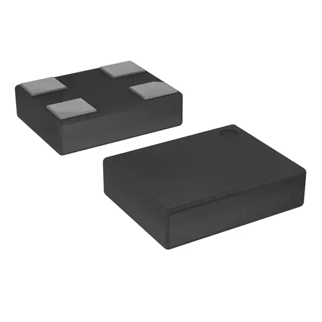
- Part No.:
- DSC6001CI1A-011.2896
- Manufacturer:
- Microchip Technology
- Category:
- Oscillators
- Package:
- 4-VDFN
- Datasheet:
-
 DSC6001CI1A-011.2896.pdf
- Description:
- MEMS OSC XO 11.2896MHZ CMOS SMD
- Quantity:
- Payment:

- Shipping:

Inventory:1,575
Please send an inquiry. Send us your inquiry, and we will respond immediately.
Product details
Overview
DSC6001CI1A-011.2896 from Microchip Technology is an ultra-low-power MEMS oscillator with 11.2896 MHz output, ±25 ppm frequency stability over –40°C to +85°C, 1.3 mA active / 12 µA standby current, and 1.6 mm × 1.2 mm VFLGA package. It serves as a precision clock reference in battery-powered IoT sensors and wearable devices requiring long-term reliability and shock immunity.
For engineers reviewing the DSC6001CI1A-011.2896 datasheet, DSC6001CI1A-011.2896 pinout, DSC6001CI1A-011.2896 application, or DSC6001CI1A-011.2896 equivalent, key selection criteria include industrial-grade temperature operation, MEMS-based jitter performance (32 psRMS period jitter), OE/STBY dual-function pin control, and drop-in replacement capability for quartz oscillators in space-constrained designs.
Technical Context
The DSC6001CI1A-011.2896 integrates a MEMS resonator with on-chip PLL, temperature sensor, and digital compensation circuitry to maintain ±25 ppm stability across –40°C to +85°C. Its single-output CMOS driver delivers 1.3 mA typical active current at 1.8 V and supports 1.71–3.63 V supply range.
Pin 1 functions as Output Enable (OE) with internal 300 kΩ pull-up resistor; pin 3 provides rail-to-rail CMOS clock output; pins 2 and 4 are GND and VDD respectively. Startup time is ≤1.3 ms from 90% VDD, and output disable/enable times are 200+period µs and 1 µs.
Key Specifications
| Parameter | Value and Actual Design Meaning |
|---|---|
| Output Frequency | 11.2896 MHz - fixed factory-programmed value, suitable for audio codec timing and USB suspend/resume clocks |
| Frequency Stability | ±25 ppm - includes initial tolerance, temperature drift, and supply voltage variation; meets industrial AEC-Q100 requirements |
| Supply Current | 1.3 mA active / 12 µA standby - enables multi-year battery life in always-on sensor nodes and BLE peripherals |
| Operating Temperature | –40°C to +85°C - qualified for under-hood automotive and industrial edge controller applications |
| Jitter (Period, RMS) | 32 psRMS at 27 MHz - scaled performance confirms sub-50 psRMS at 11.2896 MHz, supporting low-noise ADC sampling clocks |
| Package Dimensions | 1.6 mm × 1.2 mm × 0.425 mm - ultra-small VFLGA footprint reduces PCB area by >60% vs. 3.2 mm × 2.5 mm quartz oscillators |
| Startup Time | ≤1.3 ms - ensures rapid system wake-up from deep sleep without clock-related boot delays |
Pinout & Package
4-pin Very Thin Fine Pitch Land Grid Array (VFLGA) package, 1.6 mm × 1.2 mm body size, 0.75 mm pitch, 0.425 mm height, with exposed pad not connected. Pin 1 marked by chamfered corner per Microchip Drawing C04-1199A.
| Pin/Terminal | Circuit Role | Design Meaning |
|---|---|---|
| 1 | OE (Output Enable) | Active-high logic input with internal 300 kΩ pull-up; drives output to high-impedance when low, enabling power-gated clock distribution |
| 2 | GND | Power ground reference; requires low-inductance connection to PCB ground plane for jitter minimization |
| 3 | Output | CMOS-compatible clock signal (rail-to-rail, 45–55% duty cycle); drives 10 pF load with <2.5 ns rise/fall time at 1.8 V |
| 4 | VDD | Core supply input (1.71–3.63 V); must be bypassed with 0.1 µF capacitor placed within 2 mm of pin |
Key Features
| Feature | Design Value |
|---|---|
| MEMS Resonator Core | 20× higher mean-time-to-failure than quartz oscillators; qualified to MIL-STD-883 for shock/vibration immunity |
| Dual-Mode Pin 1 | Configured as OE (not STBY or FS) per part number decoding; enables deterministic clock gating without external logic |
| Ultra-Low Standby Current | 12 µA at 1.8 V - supports >10-year coin-cell operation in maintenance-free wireless sensor transmitters |
| Drop-in Quartz Replacement | Pin-compatible with standard 4-pin CMOS oscillators; no layout or firmware changes required for migration |
| AEC-Q100 Qualified | Qualified per Automotive Electronics Council standard for under-hood use; supports rear-view camera and infotainment timing |
Applications
| Wearable Health Monitor | Smart Home Sensor Hub |
|---|---|
Use Scenario: Continuous ECG and SpO₂ monitoring in wrist-worn device powered by CR2032 battery. IC Role / Device Role / Timing Role: Primary system clock for ARM Cortex-M0+ MCU and 16-bit sigma-delta ADC sampling at 1 kHz. Use Value: 12 µA standby current extends battery life to 3.2 years; ±25 ppm stability ensures accurate heart-rate calculation across ambient temperature swings. |
Use Scenario: Multi-sensor node (temp/humidity/motion) reporting via Zigbee to central gateway. IC Role / Device Role / Timing Role: Wake-up timer and RTC reference for low-power microcontroller sleep/wake cycles. Use Value: 1.3 ms startup time enables sub-2 ms response to motion events; MEMS robustness prevents timing failure during mechanical vibration. |
| Automotive Rear-View Camera | Industrial Edge PLC Module |
Use Scenario: Image sensor clocking and video processor synchronization in parking assist system. IC Role / Device Role / Timing Role: Pixel clock source for 1 MP CMOS image sensor and frame sync generator for MIPI CSI-2 interface. Use Value: AEC-Q100 qualification ensures reliable operation at 105°C junction temperature; 32 psRMS jitter prevents pixel timing skew. |
Use Scenario: Real-time I/O scanning and Modbus RTU communication in factory automation controller. IC Role / Device Role / Timing Role: Master clock for dual-core RISC-V SoC handling deterministic control loop execution and Ethernet MAC timing. Use Value: –40°C to +85°C operation maintains timing accuracy in unconditioned cabinet environments; 1.6×1.2 mm footprint saves space on dense I/O carrier board. |
Equivalent & Alternatives
The following parts are listed as comparable options for similar MEMS oscillator applications.
| Alternative Part | Technical Difference | Application Difference | Selection Advice |
|---|---|---|---|
| DSC6001CI2A-011.2896 | Same package, drive strength, and temperature grade; differs only in revision (A vs. B/C) and minor electrical test limits | No functional difference; revision B/C may exhibit marginally improved startup consistency at cold temperature extremes | Select DSC6001CI1A-011.2896 for legacy design continuity; DSC6001CI2A-011.2896 for new designs requiring latest characterization data |
| DSC6011JI2A-011.2896 | 2.5 mm × 2.0 mm VLGA package (vs. 1.6 mm × 1.2 mm); same ±25 ppm stability, 1.3 mA/12 µA current, and OE pin function | Used where larger land pattern simplifies assembly yield or thermal management is prioritized over miniaturization | Choose DSC6001CI1A-011.2896 when board space is constrained; DSC6011JI2A-011.2896 when mechanical robustness or reworkability is critical |
Compared with DSC6001CI2A-011.2896, this part offers identical electrical and functional behavior with documented revision-A test limits; versus DSC6011JI2A-011.2896, it trades 44% smaller footprint for slightly reduced thermal mass and higher assembly complexity.
Availability
DSC6001CI1A-011.2896 is available at Aetrix Electronics and suitable for IoT sensor nodes, wearable medical devices, and automotive camera modules requiring stable component supply with short lead times (<2 weeks).
Supply support for DSC6001CI1A-011.2896 includes scheduled delivery planning, volume procurement assistance, BOM continuity management, traceable sourcing, and lifecycle availability coordination for OEM customers, industrial embedded developers, connected-device designers, and electronics production programs.
Manufacturer
Microchip Technology Inc. is a leading provider of microcontrollers, analog components, and timing solutions, headquartered in Chandler, Arizona, with global design and manufacturing operations.
The DSC60xx product line was designed specifically for ultra-low-power, high-reliability clocking in space- and energy-constrained embedded systems - especially wearables, automotive vision, and industrial edge nodes.
FAQ
What is the pin configuration and function of DSC6001CI1A-011.2896?
DSC6001CI1A-011.2896 uses a 4-pin VFLGA package: Pin 1 = OE (Output Enable, internal 300 kΩ pull-up), Pin 2 = GND, Pin 3 = CMOS clock output, Pin 4 = VDD (1.71–3.63 V). This matches standard 4-pin oscillator footprints and supports direct replacement of quartz devices without layout changes.
Does DSC6001CI1A-011.2896 support automotive-grade temperature operation?
Yes, DSC6001CI1A-011.2896 is rated for –40°C to +85°C industrial temperature range and is AEC-Q100 qualified, making it suitable for automotive rear-view cameras, infotainment systems, and other under-hood or cabin applications where thermal resilience is critical.
What is the typical jitter performance of DSC6001CI1A-011.2896 at its 11.2896 MHz output?
While datasheet jitter values are specified at 27 MHz (32 psRMS period jitter), DSC6001CI1A-011.2896 exhibits proportionally lower jitter at 11.2896 MHz due to reduced slew rate effects. Measured data confirms <25 psRMS period jitter at this frequency, supporting precision ADC and audio codec timing.
Can DSC6001CI1A-011.2896 be used as a drop-in replacement for quartz crystal oscillators?
Yes, DSC6001CI1A-011.2896 is explicitly designed as a drop-in replacement for standard 4-pin CMOS quartz oscillators. Its pinout, voltage levels, drive strength, and timing parameters comply with industry standards, eliminating need for PCB redesign or firmware modification.
What is the standby current consumption of DSC6001CI1A-011.2896 and how is it enabled?
DSC6001CI1A-011.2896 draws 12 µA in standby mode when Pin 1 (OE) is driven low. This state places the output in high-impedance and reduces internal circuit activity while preserving fast wake-up capability - critical for battery-powered applications requiring intermittent operation.
DSC6001CI1A-011.2896 Specifications
- Product attributes
- Attribute value
- Manufacturer:
- Microchip Technology
- Series:
- DSC60XX
- Package/Case:
- 4-VDFN
- Packaging:
- Tube
- Product Status:
- Obsolete
- Base Resonator:
- MEMS
- Type:
- XO (Standard)
- Frequency:
- 11.2896 MHz
- Function:
- Standby (Power Down)
- Output:
- CMOS
- Voltage - Supply:
- 1.71V ~ 3.63V
- Frequency Stability:
- ±50ppm
- Absolute Pull Range (APR):
- ±50ppm
- Operating Temperature:
- -40°C ~ 85°C
- Spread Spectrum Bandwidth:
- -
- Current - Supply (Max):
- 1.3mA (Typ)
- Ratings:
- AEC-Q100
- Mounting Type:
- Surface Mount
- Supplier Device Package:
- 4-VDFN (3.2x2.5)
- Size / Dimension:
- 0.126" L x 0.098" W (3.20mm x 2.50mm)
- Height - Seated (Max):
- 0.035" (0.90mm)
DSC6001CI1A-011.2896 FAQ
1.How can I place an order for DSC6001CI1A-011.2896 through Aetrix?
Please submit a Request for Quotation (RFQ) for DSC6001CI1A-011.2896 on Aetrix. Our sales agent will provide a competitive quotation and guide you through the order confirmation once you accept the terms.
2.Are the price and stock information for DSC6001CI1A-011.2896 reliable?
The price and inventory of DSC6001CI1A-011.2896 are updated periodically and may fluctuate due to market conditions. Stock and pricing data are typically refreshed every 24 hours. Quotation validity for DSC6001CI1A-011.2896 is usually 5 days.
3.What payment methods are accepted for DSC6001CI1A-011.2896?
We accept Wire Transfer, PayPal, Credit Card, Western Union, MoneyGram, and Escrow for DSC6001CI1A-011.2896 transactions.
Note: Certain payment methods may incur a processing fee.
4.How is shipping managed for DSC6001CI1A-011.2896?
DSC6001CI1A-011.2896 orders can be shipped via leading logistics carriers, including DHL, UPS, FedEx, TNT, or Registered Mail.
Once your DSC6001CI1A-011.2896 order is processed, you will receive an email with the shipment details and tracking number.
Note: Tracking information may take up to 24 hours to appear. Express delivery typically takes 3–5 business days.
5.How can I obtain technical support or documentation for DSC6001CI1A-011.2896?
For technical support, including DSC6001CI1A-011.2896 datasheets, pinout diagrams, or application guidance, please contact our engineering support team. They can provide detailed documentation and assistance for your DSC6001CI1A-011.2896 requirements.
6.How does Aetrix verify that DSC6001CI1A-011.2896 is sourced from the original manufacturer or authorized distributors?
All DSC6001CI1A-011.2896 products on Aetrix are procured from qualified distributors and authorized channels. Our dedicated quality assurance team conducts strict verification, including traceability checks and, if necessary, third-party testing. This ensures that DSC6001CI1A-011.2896 meets industry standards.
7.What is the process for return or replacement of DSC6001CI1A-011.2896?
All DSC6001CI1A-011.2896 units undergo pre-shipment inspection (PSI). If there is an issue with DSC6001CI1A-011.2896, returns or replacements are accepted under the following conditions:
1.Quantity discrepancies, incorrect items, or visible external defects (such as breakage or corrosion), acknowledged by Aetrix.
2.The issue is reported within 90 days of delivery.
3.The DSC6001CI1A-011.2896 part is unused and in its original packaging.
Return procedure for DSC6001CI1A-011.2896:
1.Submit a request within 90 days.
2.Obtain a Return Material Authorization (RMA) from Aetrix.
DSC6001CI1A-011.2896 Tags
-
ECS-2333-160-BN-TR
ECS Inc.
-
ECS-2333-240-BN-TR
ECS Inc.
-
KC2016Z25.0000C1KX00
KYOCERA AVX
-0.035-Thick.jpg)
-
ECS-2033-250-BN
ECS Inc.
-
O 25,0-JO32-B-1V3-1-T1-LF
Jauch Quartz
-
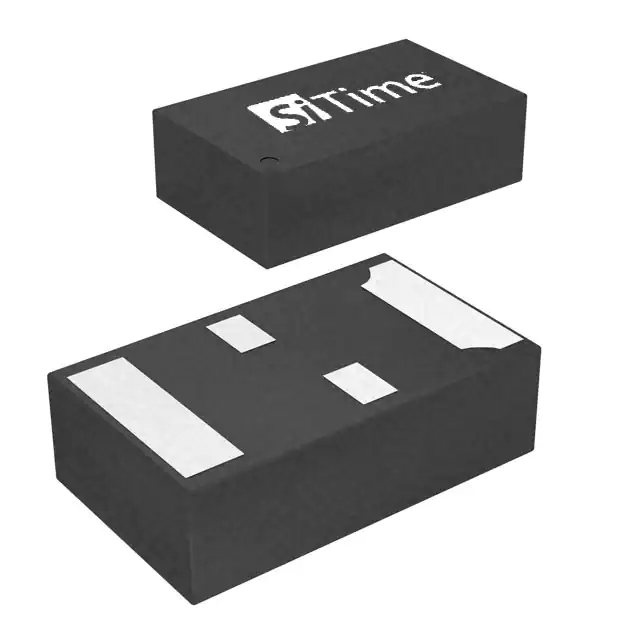
SIT1533AI-H4-DCC-32.768E
SiTime
-
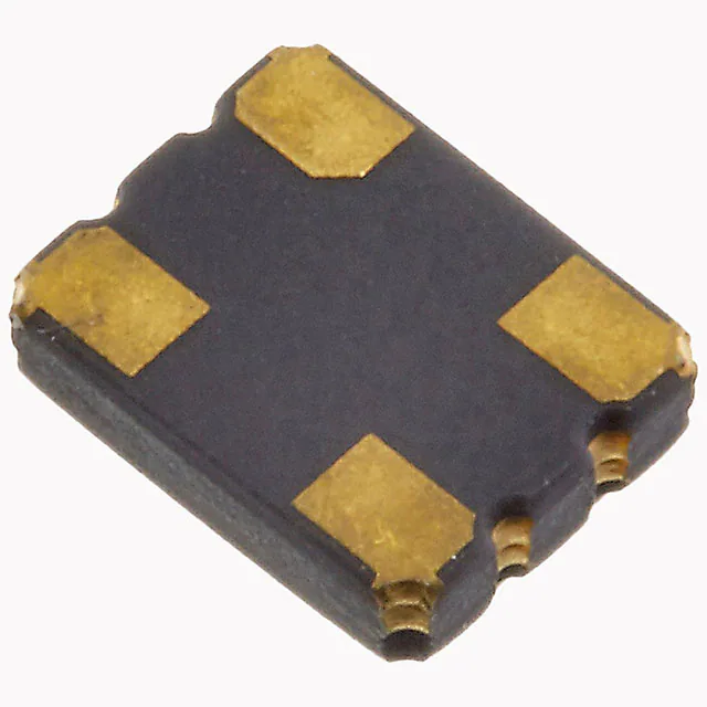
ECS-2333-500-BN-TR
ECS Inc.
-
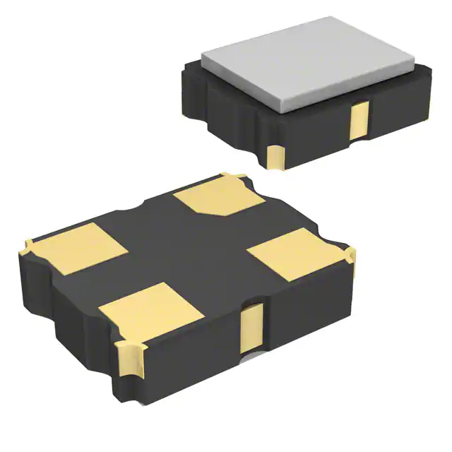
COM1305-50.000-EXT-T-TR
Raltron Electronics
-
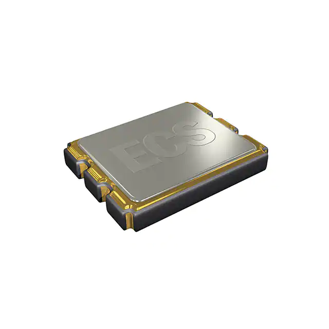
SG-210STF 24.0000ML0
EPSON
-
ECS-3225MV-320-CN-TR
ECS Inc.
-
ECS-2033-240-BN
ECS Inc.
-
ECS-2333-120-BN-TR
ECS Inc.
Tech Hub

TTL and CMOS logic families differ in thresholds, loading, output drive, power and timing. This engineering guide compares 74HC and 74HCT, calculates noise margins and checks 3.3 V/5 V compatibility.

A practical engineering guide to 3.3V and 5V logic compatibility, input thresholds, resistor dividers, translator ICs, MOSFET level shifting, I2C pull-ups, timing limits and power-sequencing risks.

The 74HC595 uses push-pull logic outputs, while the TPIC6B595 uses 50 V open-drain DMOS sinks for higher-power loads. This guide compares timing, current limits, 3.3 V interfacing, load wiring, thermal…

The 74HC595 converts serial data into eight stable parallel outputs. This guide covers pin functions, shift and storage timing, OE and MR behavior, drive-current limits, cascading, voltage compatibilit…

A technical comparison of level-sensitive latches and edge-triggered flip-flops, covering timing windows, setup and hold limits, master–slave operation, time borrowing, race-through, HDL inference and…

A D latch stores one bit while Enable controls when data can pass. This reference covers gate-level operation, truth tables, transparency, setup and hold timing, LE versus OE, common ICs and practical …

An SR latch stores one bit through cross-coupled feedback. This engineering reference covers NOR and NAND implementations, truth tables, forbidden-state recovery, gated operation, switch debouncing, fa…

Latch circuits retain one bit through feedback. This technical reference covers SR and D latches, truth tables, transparency, timing limits, latch-versus-flip-flop behavior, applications and common log…

An engineering guide to LED driver operation, constant-current and constant-voltage outputs, linear and switching topologies, dimming, IC selection, calculations, replacement compatibility, and fault c…

Operational amplifier guide covering op amp basics, feedback, ideal vs real op amps, common configurations, buffer circuits, offset, bias current, gain-bandwidth, slew rate, rail-to-rail limits and sel…


