
 My Inquiry
 My Account


STMicroelectronics DSM2190F4V-15K6
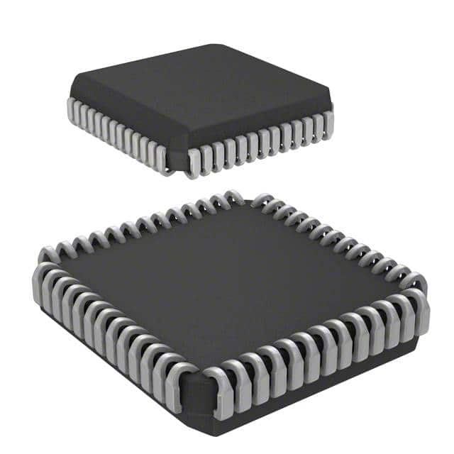
- Part No.:
- DSM2190F4V-15K6
- Manufacturer:
- STMicroelectronics
- Category:
- Memory
- Package:
- 52-LCC (J-Lead)
- Datasheet:
-
 DSM2190F4V-15K6.pdf
- Description:
- IC FLASH 2MBIT PARALLEL 52PLCC
- Quantity:
- Payment:

- Shipping:

Inventory:3,528
Please send an inquiry. Send us your inquiry, and we will respond immediately.
Product details
Overview
DSM2190F4V-15K6 from STMicroelectronics is a Digital Signal Processor System Memory (DSM) device designed for seamless, glueless integration with Analog Devices ADSP-2191 DSPs operating at 3.3 V. It integrates dual Flash memory arrays (256K × 8 main + 32K × 8 secondary), a 3,000-gate CPLD with 16 macrocells, up to 16 multifunction I/O pins, and JTAG-based in-system programming - enabling concurrent code/data access, boot-from-external-memory operation, and field-upgradable logic and firmware.
For engineers reviewing the DSM2190F4V-15K6 datasheet, DSM2190F4V-15K6 pinout, DSM2190F4V-15K6 application, or DSM2190F4V-15K6 equivalent, key selection criteria include its 150 ns Flash access time, sector-wise write protection, zero-power standby current (25 µA), PLCC52 package compatibility with ADSP-2191 address/data/control bus, and runtime-configurable decode PLD for flexible memory mapping.
Technical Context
The DSM2190F4V-15K6 implements a two-chip DSP system architecture where the ADSP-2191 interfaces directly via 22-bit address, 8-bit data, and control signals (BMS, IOMS, MSx) without external glue logic. Its Decode PLD (DPLD) dynamically maps Flash sectors to any address boundary using programmable address decoding logic, supporting bootloading, code swapping, and parameter storage.
The integrated CPLD contains 16 output macrocells (OMCs) with direct DSP data bus access for real-time peripheral emulation (e.g., shifters, counters, state machines), while input macrocells (IMCs) condition Port B/C signals for debouncing or synchronous sampling - all configurable via JTAG ISP alongside Flash and security bits.
Key Specifications
| Parameter | Value and Actual Design Meaning |
|---|---|
| Main Flash Capacity | 256K × 8 (8 sectors × 32 KB): Enables full DSP boot code + application code storage with sector-level erasure. |
| Secondary Flash Capacity | 32K × 8 (4 sectors × 8 KB): Supports calibration constants, startup routines, or EEPROM-emulated data logging. |
| Flash Access Time | 150 ns: Matches ADSP-2191's external memory timing requirements for zero-wait-state operation. |
| PLD Resources | 3,000 gates + 16 macrocells: Sufficient for chip selects, clock dividers, keypad interfaces, and simple state machines. |
| Supply & Temp Range | 3.3 V ±10%, –40°C to +85°C: Industrial-grade operation compatible with ADSP-2191's I/O voltage and thermal envelope. |
| Standby Current | 25 µA: Enables battery-powered DSP systems with ultra-low power retention between memory/logic accesses. |
| JTAG ISP Time | 10–25 seconds: Allows full device programming (Flash + PLD + security) offline, eliminating DSP involvement in manufacturing. |
Pinout & Package
DSM2190F4V-15K6 is housed in a 52-pin PLCC (Plastic Leaded Chip Carrier) package with gull-wing leads, optimized for through-hole mounting and thermal reliability in industrial DSP applications.
| Pin/Terminal | Circuit Role | Design Meaning |
|---|---|---|
| AD0–AD7 | DSP Data Bus Interface | 8-bit bidirectional data path to ADSP-2191; carries Flash reads/writes and PLD register transfers. |
| A0–A21 | DSP Address Bus Interface | 22-bit address lines decoded by DPLD to select Flash sectors or control registers. |
| BMS, IOMS, MS0–MS3 | DSP Memory Strobe Inputs | Glueless interface: BMS/IOMS enable memory-mapped access; MSx support sector-select decoding. |
| PD0–PD7, PC0–PC7, PB0–PB7 | Multifunction I/O Ports | 16 configurable pins - driven by DSP software or CPLD logic; support chip selects, flags, or peripheral interfacing. |
| TCK, TMS, TDI, TDO | JTAG ISP Boundary Scan | Full in-system programming of Flash, PLD, and security bit without DSP boot or runtime intervention. |
| VCC, GND | Power Supply | Single 3.3 V supply with dedicated ground pins; supports zero-power mode during idle cycles. |
Key Features
| Feature | Design Value |
|---|---|
| Dual independent Flash banks | Enables concurrent read-while-erase: DSP executes from Main Flash while updating Secondary Flash with new calibration data. |
| Sector-level write protection | Each 32 KB (Main) or 8 KB (Secondary) Flash sector can be locked independently - preserving boot code integrity against accidental overwrite. |
| Runtime-accessible PLD macrocells | 16 OMCs directly mapped to DSP data bus allow real-time read/write of counter states or shifter positions without interrupt overhead. |
| Programmable security bit | Blocks external JTAG access to Flash/PLD contents; DSP retains full read access to Flash - enabling secure field deployment with debug visibility. |
| Zero-power standby mode | Automatic transition to 25 µA sleep state between memory accesses or PLD input transitions - critical for portable DSP instrumentation. |
Applications
| Audio Signal Processing | Industrial Motor Control |
|---|---|
Use Scenario: Real-time FIR filtering and dynamic range compression in portable audio analyzers. IC Role / Device Role / Timing Role: DSM2190F4V-15K6 stores filter coefficient tables and runtime-adjustable gain parameters in protected Flash sectors, while CPLD generates precise PWM dead-time logic synchronized to DSP timer outputs. Use Value: Eliminates external SRAM and discrete logic; enables field updates to audio algorithms without hardware revision. | Use Scenario: Closed-loop servo drive with adaptive commutation timing and fault logging. IC Role / Device Role / Timing Role: Stores motor profile lookup tables in Main Flash and captures encoder error logs in Secondary Flash; CPLD implements hardware-based overcurrent shutdown with <100 ns response. Use Value: Reduces BOM count by replacing discrete EEPROM + CPLD + level shifters; supports Just-In-Time firmware loading during production test. |
| Medical Ultrasound Beamforming | Test & Measurement Equipment |
Use Scenario: High-channel-count beamformer requiring calibrated delay profiles and real-time gain compensation. IC Role / Device Role / Timing Role: Holds channel-specific calibration constants in 8 KB Secondary Flash sectors; DSP loads them on demand via BMS-strobed reads while executing beamforming kernels from Main Flash. Use Value: Sector granularity allows per-probe calibration updates without reprogramming entire firmware image. | Use Scenario: Portable oscilloscope with firmware-upgradable trigger algorithms and waveform storage. IC Role / Device Role / Timing Role: Stores oscilloscope firmware in Main Flash and user-defined math functions in Secondary Flash; JTAG ISP enables lab-based algorithm iteration without board rework. Use Value: 10–25 second ISP cycle accelerates validation of new trigger logic; zero-power mode extends battery life during idle capture. |
Equivalent & Alternatives
The following parts are listed as comparable options for similar DSP system memory applications.
| Alternative Part | Technical Difference | Application Difference | Selection Advice |
|---|---|---|---|
| DSM2190F4VV-15T6 | Same Flash/PLD/I/O specs but PQFP52 package instead of PLCC52; 150 ns speed grade identical. | Preferred for surface-mount assembly lines; lacks PLCC's mechanical robustness and thermal mass for high-vibration environments. | Select for automated SMT production; avoid if board requires through-hole mounting or higher thermal cycling tolerance. |
| ST M29W256GL | Standalone 256 Mb parallel NOR Flash (no PLD, no I/O, no JTAG ISP); 90 ns access, 3.0–3.6 V supply. | Requires external address decoder and CPLD for ADSP-2191 interface; no in-system logic reconfiguration capability. | Choose only when Flash-only expansion is needed and discrete logic resources are already available on board. |
Compared with DSM2190F4V-15K6, the PQFP variant offers SMT compatibility but sacrifices mechanical ruggedness, while the standalone M29W256GL delivers faster access but forces designers to replicate decode logic, I/O expansion, and secure programming infrastructure externally - increasing BOM, layout complexity, and qualification effort.
Availability
DSM2190F4V-15K6 is available at Aetrix Electronics and suitable for audio signal processing, industrial motor control, medical ultrasound beamforming, and test & measurement equipment requiring stable component supply across extended temperature ranges and long product lifecycles.
Supply support for DSM2190F4V-15K6 includes scheduled delivery planning, volume procurement assistance, BOM continuity management, traceable sourcing, and lifecycle availability coordination for OEM customers, industrial embedded developers, connected-device designers, and electronics production programs.
Manufacturer
STMicroelectronics is a global semiconductor leader specializing in microcontrollers, analog ICs, and memory solutions for industrial, automotive, and consumer applications.
The DSM family was engineered specifically to simplify ADSP-2191-based designs by integrating Flash, PLD, and I/O into a single programmable system memory device - reducing component count, PCB area, and development time for DSP-centric embedded systems.
FAQ
What is the role of the Decode PLD (DPLD) in DSM2190F4V-15K6?
The Decode PLD (DPLD) dynamically maps individual Flash memory sectors - both Main (8 × 32 KB) and Secondary (4 × 8 KB) - to any address boundary within the ADSP-2191's memory space. It uses DSP address and control signals (e.g., BMS, MSx) to generate sector-select outputs, enabling flexible boot configurations, code swapping, and parameter storage without external logic. DPLD also drives external chip selects on Port D pins.
Can DSM2190F4V-15K6 execute code directly from Flash memory upon DSP reset?
Yes. The DSM2190F4V-15K6 supports boot-from-external-memory operation: the ADSP-2191 can be configured to fetch its initial instruction stream directly from Main or Secondary Flash. Custom startup code may be stored in Secondary Flash sectors and executed immediately after reset, freeing Main Flash for application code and enabling clean software partitioning.
How does the security bit protect intellectual property on DSM2190F4V-15K6?
When enabled, the programmable security bit blocks all external JTAG programming tools (including FlashLINK™ cable) from reading or writing Flash contents and PLD configuration. The ADSP-2191 retains full read access to Flash memory for runtime execution, preserving functionality while preventing unauthorized firmware extraction or cloning. Security can only be disabled by performing a full chip erase.
Is DSM2190F4V-15K6 compatible with other ADSP processors besides ADSP-2191?
No. DSM2190F4V-15K6 is specifically architected for the ADSP-2191's external port timing, strobe signaling (BMS/IOMS/MSx), and 22-bit address/8-bit data bus structure. Its decode logic, PLD interface, and runtime register map are not compatible with ADSP-218x, ADSP-2196, or SHARC families - confirmed by ST's documentation and Analog Devices' hardware reference manual.
DSM2190F4V-15K6 Specifications
- Product attributes
- Attribute value
- Manufacturer:
- STMicroelectronics
- Series:
- -
- Package/Case:
- 52-LCC (J-Lead)
- Packaging:
- Tube
- Product Status:
- Obsolete
- Programmable:
- Not Verified
- Memory Type:
- Non-Volatile
- Memory Format:
- FLASH
- Technology:
- FLASH
- Memory Size:
- 2Mbit
- Memory Organization:
- 256K x 8
- Memory Interface:
- Parallel
- Clock Frequency:
- -
- Write Cycle Time - Word, Page:
- -
- Access Time:
- 150 ns
- Voltage - Supply:
- 3V ~ 3.6V
- Operating Temperature:
- -40°C ~ 85°C (TA)
- Grade:
- -
- Qualification:
- -
- Mounting Type:
- Surface Mount
- Supplier Device Package:
- 52-PLCC (19.1x19.1)
DSM2190F4V-15K6 FAQ
1.How can I place an order for DSM2190F4V-15K6 through Aetrix?
Please submit a Request for Quotation (RFQ) for DSM2190F4V-15K6 on Aetrix. Our sales agent will provide a competitive quotation and guide you through the order confirmation once you accept the terms.
2.Are the price and stock information for DSM2190F4V-15K6 reliable?
The price and inventory of DSM2190F4V-15K6 are updated periodically and may fluctuate due to market conditions. Stock and pricing data are typically refreshed every 24 hours. Quotation validity for DSM2190F4V-15K6 is usually 5 days.
3.What payment methods are accepted for DSM2190F4V-15K6?
We accept Wire Transfer, PayPal, Credit Card, Western Union, MoneyGram, and Escrow for DSM2190F4V-15K6 transactions.
Note: Certain payment methods may incur a processing fee.
4.How is shipping managed for DSM2190F4V-15K6?
DSM2190F4V-15K6 orders can be shipped via leading logistics carriers, including DHL, UPS, FedEx, TNT, or Registered Mail.
Once your DSM2190F4V-15K6 order is processed, you will receive an email with the shipment details and tracking number.
Note: Tracking information may take up to 24 hours to appear. Express delivery typically takes 3–5 business days.
5.How can I obtain technical support or documentation for DSM2190F4V-15K6?
For technical support, including DSM2190F4V-15K6 datasheets, pinout diagrams, or application guidance, please contact our engineering support team. They can provide detailed documentation and assistance for your DSM2190F4V-15K6 requirements.
6.How does Aetrix verify that DSM2190F4V-15K6 is sourced from the original manufacturer or authorized distributors?
All DSM2190F4V-15K6 products on Aetrix are procured from qualified distributors and authorized channels. Our dedicated quality assurance team conducts strict verification, including traceability checks and, if necessary, third-party testing. This ensures that DSM2190F4V-15K6 meets industry standards.
7.What is the process for return or replacement of DSM2190F4V-15K6?
All DSM2190F4V-15K6 units undergo pre-shipment inspection (PSI). If there is an issue with DSM2190F4V-15K6, returns or replacements are accepted under the following conditions:
1.Quantity discrepancies, incorrect items, or visible external defects (such as breakage or corrosion), acknowledged by Aetrix.
2.The issue is reported within 90 days of delivery.
3.The DSM2190F4V-15K6 part is unused and in its original packaging.
Return procedure for DSM2190F4V-15K6:
1.Submit a request within 90 days.
2.Obtain a Return Material Authorization (RMA) from Aetrix.
DSM2190F4V-15K6 Tags

-
M24C02-WMN6TP
STMicroelectronics

-
AT24C02C-XHM-T
Microchip Technology

-
AT21CS01-STUM10-T
Microchip Technology

-
AT24C02C-SSHM-T
Microchip Technology

-
24LC01BT-I/OT
Microchip Technology

-
M24C02-FMC6TG
STMicroelectronics
-
AT24CS02-SSHM-T
Microchip Technology

-
93LC46BT-I/OT
Microchip Technology
-
AT24C04C-SSHM-T
Microchip Technology

-
24LC01BT-I/SN
Microchip Technology
-
24AA02UIDT-I/OT
Microchip Technology

-
AT24C08C-STUM-T
Microchip Technology
Tech Hub

A practical engineering and sourcing framework covering lifecycle verification, lifetime-buy calculations, replacement qualification, supplier checks and counterfeit-risk controls.

TTL and CMOS logic families differ in thresholds, loading, output drive, power and timing. This engineering guide compares 74HC and 74HCT, calculates noise margins and checks 3.3 V/5 V compatibility.

A practical engineering guide to 3.3V and 5V logic compatibility, input thresholds, resistor dividers, translator ICs, MOSFET level shifting, I2C pull-ups, timing limits and power-sequencing risks.

The 74HC595 uses push-pull logic outputs, while the TPIC6B595 uses 50 V open-drain DMOS sinks for higher-power loads. This guide compares timing, current limits, 3.3 V interfacing, load wiring, thermal…

The 74HC595 converts serial data into eight stable parallel outputs. This guide covers pin functions, shift and storage timing, OE and MR behavior, drive-current limits, cascading, voltage compatibilit…

A technical comparison of level-sensitive latches and edge-triggered flip-flops, covering timing windows, setup and hold limits, master–slave operation, time borrowing, race-through, HDL inference and…

A D latch stores one bit while Enable controls when data can pass. This reference covers gate-level operation, truth tables, transparency, setup and hold timing, LE versus OE, common ICs and practical …

An SR latch stores one bit through cross-coupled feedback. This engineering reference covers NOR and NAND implementations, truth tables, forbidden-state recovery, gated operation, switch debouncing, fa…

Latch circuits retain one bit through feedback. This technical reference covers SR and D latches, truth tables, transparency, timing limits, latch-versus-flip-flop behavior, applications and common log…

An engineering guide to LED driver operation, constant-current and constant-voltage outputs, linear and switching topologies, dimming, IC selection, calculations, replacement compatibility, and fault c…


