
 My Inquiry
 My Account


NXP Semiconductors DSPB56374AE
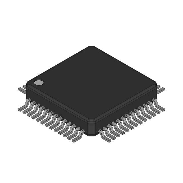
- Part No.:
- DSPB56374AE
- Manufacturer:
- NXP Semiconductors
- Category:
- DSP (Digital Signal Processors)
- Package:
- 52-LQFP
- Datasheet:
-
 DSPB56374AE.pdf
- Description:
- IC DSP 24BIT 150MHZ 52-LQFP
- Quantity:
- Payment:

- Shipping:

Inventory:1,981
Please send an inquiry. Send us your inquiry, and we will respond immediately.
Product details
Overview
DSPB56374AE from Freescale Semiconductor is a 24-bit programmable digital signal processor (DSP) optimized for real-time audio processing, featuring a 150 MHz internal clock, 150 MIPS performance, 6K×24-bit X/Y data RAM, 20K×24-bit program ROM, and dual Enhanced Serial Audio Interfaces (ESAI/ESAI_1) supporting I2S, AC97, and Sony protocols in automotive infotainment systems.
For engineers reviewing the DSPB56374AE datasheet, DSPB56374AE pinout, DSPB56374AE application, or DSPB56374AE equivalent, key selection criteria include its 80-pin LQFP package, 1.25 V core / 3.3 V I/O supply architecture, six-channel DMA, triple timer module, and GPIO-configurable pins-critical for audio subsystem integration, acoustic equalization, and multi-channel sound field processing.
Technical Context
The DSPB56374AE implements the DSP56300 core with object-code compatibility to the 56K family, integrating a 24×24-bit MAC unit, 56-bit barrel shifter, and two 56-bit accumulators. Its memory architecture supports flexible switching between 2K–10K program RAM and 4K–10K X-data RAM configurations via MSW bits.
It features dual ESAI peripherals-one standard (ESAI) and one enhanced (ESAI_1, 80-pin only)-each supporting up to 6 transmitters and 4 receivers with master/slave operation. The SHI interface provides SPI/I²C dual-mode host connectivity with 10-word FIFO and three noise-reduction filter modes.
Key Specifications
| Parameter | Value and Actual Design Meaning |
|---|---|
| Core Architecture | DSP56300 24-bit fixed-point core, object-code compatible with 56K family |
| Performance | 150 MIPS at 150 MHz internal clock; enables real-time execution of complex FIR/IIR filters and FFTs |
| Memory Configuration | 6K×24-bit X/Y Data RAM + 20K×24-bit Program/Bootstrap ROM + configurable memory switches |
| ESAI Interfaces | ESAI (12-pin) + ESAI_1 (12-pin, 80-pin package only); supports I2S, AC97, Sony, network protocols |
| Serial Host Interface | SHI with SPI/I²C dual-mode support, 10-word receive FIFO, 8/16/24-bit word length |
| Power Supply | 1.25 V core (CORE_VDD/PLLD_VDD) + 3.3 V I/O (IO_VDD); 5 V-tolerant GPIO on MOD/IRQ pins |
| Package | 80-pin LQFP (12×12 mm, 0.5 mm pitch); pin-compatible with DSP56374 family variants |
Pinout & Package
Package: 80-pin LQFP (12 mm × 12 mm, 0.5 mm pitch), thermally enhanced with exposed pad. Designed for high-density audio PCB layouts requiring low-noise analog/digital partitioning and robust power decoupling per PLLA/PLLP/PLLD/CORE/IO domains.
| Pin/Terminal | Circuit Role | Design Meaning |
|---|---|---|
| EXTAL | External Clock Input | Accepts crystal or external clock source (1–50 MHz) to drive internal PLL; required during RESET assertion |
| PINIT/NMI | PLL Init / NMI Input | Latches PLL enable state at reset; serves as negative-edge-triggered nonmaskable interrupt during operation |
| RESET | Active-Low Reset Input | Schmitt-triggered, 5 V tolerant; must be asserted during power-up with stable EXTAL present |
| HCKR / HCKT | ESAI High-Freq Clock I/O | Configurable as input (receiver/transmitter clock source) or output (sample clock for external DAC/ADC) |
| FSR / FST | ESAI Frame Sync I/O | Asynchronous/synchronous frame sync control; direction set by RFSD/TFSD bits in RCCR/TCCR registers |
| SDO0–SDO5 / SDI0–SDI1 | ESAI Serial Data I/O | Up to 6 transmitters and 4 receivers; each mapped to dedicated port C pins (PC0–PC7) with GPIO fallback |
| MODA–MODD | Mode Select / IRQ Inputs | 5 V tolerant Schmitt-trigger inputs; select 1 of 16 boot modes and serve as maskable interrupt sources |
| PH0–PH4 / PC0–PC7 / PG0–PG14 | GPIO Ports | 47 total programmable GPIOs (80-pin package); individually configurable as input/output/disconnected with pull-up/down |
Key Features
| Feature | Design Value |
|---|---|
| Triple Timer Module (TEC) | Three independent 16-bit timers with capture/compare/PWM capability for audio synchronization and system timing |
| Hardware Watchdog Timer | Dedicated watchdog with timeout configuration; resets device if software fails to service it within programmed interval |
| JTAG/OnCE Debug Support | IEEE 1149.1-compliant boundary scan + OnCE real-time debug interface for hardware/software co-verification |
| Low-Power Operation | STOP/WAIT standby modes; static CMOS design enabling DC operation; clock divider reduces EMI in sensitive audio bands |
| Flexible Memory Mapping | MSW-controlled memory switch allows runtime reconfiguration of program/data RAM sizes without external memory |
Applications
| Automotive Infotainment Head Unit | Professional Audio Mixer |
|---|---|
Use Scenario: Multi-source audio routing, surround sound decoding, and real-time parametric EQ in vehicle head units with Bluetooth, USB, and tuner inputs. IC Role / Device Role / Timing Role: Primary audio DSP executing Dolby Pro Logic II, DTS Neural:X, and speaker time-alignment algorithms with sub-10 µs latency. Use Value: Dual ESAI interfaces enable simultaneous connection to multiple codecs (e.g., TI PCM3060 + AKM AK4118), while 150 MIPS ensures headroom for future firmware upgrades. | Use Scenario: Digital mixing console with 32-channel input, dynamic processing, and effects rendering for live sound reinforcement. IC Role / Device Role / Timing Role: Central signal processor handling channel strip dynamics (compressor/limiter), harmonic excitation, and stereo imaging in parallel pipelines. Use Value: Six-channel DMA offloads data movement from core, preserving MIPS for compute-intensive algorithms; SHI enables host MCU control over gain/pan parameters via I²C. |
| Home Theater AV Receiver | Industrial Audio Analytics Node |
Use Scenario: 7.1-channel decoding, bass management, room correction (Audyssey MultEQ), and HDMI audio passthrough in premium AV receivers. IC Role / Device Role / Timing Role: Secondary DSP co-processing alongside main SoC, managing real-time FIR-based room compensation filters updated per microphone sweep. Use Value: 20K×24-bit bootstrap ROM stores factory calibration data and recovery firmware; ESAI_1 supports auxiliary ADC/DAC for measurement loopback. | Use Scenario: Edge-based acoustic monitoring in manufacturing plants detecting bearing faults or weld integrity via spectral anomaly detection. IC Role / Device Role / Timing Role: Standalone audio analytics engine capturing vibration signatures via MEMS microphones and running FFT + machine learning inference kernels. Use Value: STOP mode reduces power to <1 mW during idle; GPIOs interface directly with industrial sensors and RS-485 transceivers for Modbus RTU reporting. |
Equivalent & Alternatives
The following parts are listed as comparable options for similar digital audio DSP applications.
| Alternative Part | Technical Difference | Application Difference | Selection Advice |
|---|---|---|---|
| MC56F8323 | 16-bit DSC with 60 MIPS, integrated flash, no ESAI; uses SCI/SPI instead of SHI/ESAI | Limited to basic audio control (volume/tone), not suitable for multi-channel codec interfacing or real-time filtering | Select when cost-sensitive motor+audio combo control is needed, not full audio DSP functionality |
| ADSP-21369 | 32-bit SHARC DSP, 400 MHz, 2400 MMAC, 512K words internal RAM; lacks native AC97/I2S support | Requires external interface logic for audio codecs; superior for floating-point math but over-specified for fixed-point audio tasks | Select for floating-point beamforming or radar-audio fusion; avoid if I2S/AC97 direct-connect is mandatory |
Compared with MC56F8323 and ADSP-21369, the DSPB56374AE uniquely balances 24-bit fixed-point precision, dual native ESAI support, and 150 MIPS at low power-making it optimal for cost-constrained, high-channel-count audio systems requiring zero-latency codec interfacing without external glue logic.
Availability
DSPB56374AE is available at Aetrix Electronics and suitable for automotive infotainment, professional audio equipment, and home theater AV receivers requiring stable component supply across extended product lifecycles.
Supply support for DSPB56374AE includes scheduled delivery planning, volume procurement assistance, BOM continuity management, traceable sourcing, and lifecycle availability coordination for OEM customers, industrial embedded developers, connected-device designers, and electronics production programs.
Manufacturer
Freescale Semiconductor (now part of NXP Semiconductors) is a fabless semiconductor company specializing in embedded processing, analog, and connectivity solutions for automotive, industrial, and consumer markets.
The DSP56374AE belongs to the Symphony™ DSP family, designed specifically for high-fidelity digital audio signal processing in resource-constrained, real-time embedded systems with stringent EMI and thermal requirements.
FAQ
What is the maximum operating frequency of the DSPB56374AE core?
The DSPB56374AE operates at a maximum internal clock frequency of 150 MHz, delivering 150 million instructions per second (MIPS). This frequency is generated internally via the integrated PLL using an external crystal or clock source applied to the EXTAL pin. The core logic supply (CORE_VDD) must be stabilized at 1.25 V to sustain this performance level, and the PLL requires separate 1.25 V (PLLD_VDD) and 3.3 V (PLLA_VDD/PLLP_VDD) supplies with strict decoupling.
Does the DSPB56374AE support I²S protocol natively?
Yes, the DSPB56374AE supports I²S natively through both its Enhanced Serial Audio Interface (ESAI) and ESAI_1 peripherals. Each interface can be configured as master or slave and supports I²S, AC97, Sony, and network protocols. The ESAI_1 module is available only in the 80-pin LQFP package and provides additional flexibility for multi-codec systems. Frame sync (FSR/FST) and serial clock (SCKR/SCKT) pins are fully programmable to match I²S timing requirements including left/right justification and delay settings.
How many GPIO pins are available on the DSPB56374AE in the 80-pin package?
The DSPB56374AE provides up to 47 general-purpose I/O pins in the 80-pin LQFP package. These are distributed across Port G (15 dedicated GPIO), Port H (5 multiplexed with MOD/IRQ), and Port C (up to 27 multiplexed with ESAI functions). All GPIOs are individually configurable as input, output, or high-impedance disconnected, with internal pull-up or pull-down resistors enabled per pin. MODA–MODD pins are 5 V tolerant and retain GPIO capability after boot mode selection.
What debug interfaces does the DSPB56374AE include?
The DSPB56374AE integrates IEEE 1149.1-compliant JTAG boundary scan and the OnCE (On-Chip Emulation) interface for real-time hardware/software debugging. OnCE supports breakpoints, watchpoints, register inspection, and memory access without halting real-time audio processing. The JTAG port enables board-level test and programming, while the SHI interface can also be used for host-based firmware updates. No external debug probe is required beyond standard JTAG cabling for full visibility into core state and peripheral registers.
Is the DSPB56374AE pin-compatible with other devices in the DSP56374 family?
Yes, the DSPB56374AE is pin-compatible with the base DSP56374 in the 80-pin LQFP package, sharing identical pin assignments, power domains, and signal groupings. Differences between variants (e.g., DSP56374AF, DSPB56374AE) relate to mask-set revisions, characterization grade (industrial vs. automotive), and minor electrical parameter tolerances-not pinout or functional interface behavior. Designers may substitute within the same package variant without PCB changes, provided thermal and power delivery meet the specific variant's datasheet specifications.
DSPB56374AE Specifications
- Product attributes
- Attribute value
- Manufacturer:
- NXP Semiconductors
- Series:
- DSP56K/Symphony
- Package/Case:
- 52-LQFP
- Packaging:
- Tray
- Product Status:
- Not For New Designs
- Type:
- Audio Processor
- Interface:
- Host Interface, I2C, SAI, SPI
- Clock Rate:
- 150MHz
- Non-Volatile Memory:
- ROM (84kB)
- On-Chip RAM:
- 54kB
- Voltage - I/O:
- 3.30V
- Voltage - Core:
- 1.25V
- Operating Temperature:
- 0°C ~ 70°C (TA)
- Grade:
- -
- Qualification:
- -
- Mounting Type:
- Surface Mount
- Supplier Device Package:
- 52-TQFP (10x10)
DSPB56374AE FAQ
1.How can I place an order for DSPB56374AE through Aetrix?
Please submit a Request for Quotation (RFQ) for DSPB56374AE on Aetrix. Our sales agent will provide a competitive quotation and guide you through the order confirmation once you accept the terms.
2.Are the price and stock information for DSPB56374AE reliable?
The price and inventory of DSPB56374AE are updated periodically and may fluctuate due to market conditions. Stock and pricing data are typically refreshed every 24 hours. Quotation validity for DSPB56374AE is usually 5 days.
3.What payment methods are accepted for DSPB56374AE?
We accept Wire Transfer, PayPal, Credit Card, Western Union, MoneyGram, and Escrow for DSPB56374AE transactions.
Note: Certain payment methods may incur a processing fee.
4.How is shipping managed for DSPB56374AE?
DSPB56374AE orders can be shipped via leading logistics carriers, including DHL, UPS, FedEx, TNT, or Registered Mail.
Once your DSPB56374AE order is processed, you will receive an email with the shipment details and tracking number.
Note: Tracking information may take up to 24 hours to appear. Express delivery typically takes 3–5 business days.
5.How can I obtain technical support or documentation for DSPB56374AE?
For technical support, including DSPB56374AE datasheets, pinout diagrams, or application guidance, please contact our engineering support team. They can provide detailed documentation and assistance for your DSPB56374AE requirements.
6.How does Aetrix verify that DSPB56374AE is sourced from the original manufacturer or authorized distributors?
All DSPB56374AE products on Aetrix are procured from qualified distributors and authorized channels. Our dedicated quality assurance team conducts strict verification, including traceability checks and, if necessary, third-party testing. This ensures that DSPB56374AE meets industry standards.
7.What is the process for return or replacement of DSPB56374AE?
All DSPB56374AE units undergo pre-shipment inspection (PSI). If there is an issue with DSPB56374AE, returns or replacements are accepted under the following conditions:
1.Quantity discrepancies, incorrect items, or visible external defects (such as breakage or corrosion), acknowledged by Aetrix.
2.The issue is reported within 90 days of delivery.
3.The DSPB56374AE part is unused and in its original packaging.
Return procedure for DSPB56374AE:
1.Submit a request within 90 days.
2.Obtain a Return Material Authorization (RMA) from Aetrix.
DSPB56374AE Tags
-
TMS320C5535AZAY10
Texas Instruments
-
TMS320VC5501PGF300
Texas Instruments
-
ADSP-BF592KCPZ
Analog Devices Inc.
-
ADAU1463WBCPZ150
Analog Devices Inc.

-
TMS320VC5402PGE100
Texas Instruments

-
ADAU1701JSTZ-RL
Analog Devices Inc.
-
ADAU1701JSTZ
Analog Devices Inc.
-
TMS320VC5502PGF300
Texas Instruments
-
ADAU1462WBCPZ300RL
Analog Devices Inc.
-
ADAU1452KCPZRL
Analog Devices Inc.
-
ADAU1452WBCPZ-RL
Analog Devices Inc.
-
TMS320C6747DZKB3
Texas Instruments
Tech Hub

A practical engineering guide to 3.3V and 5V logic compatibility, input thresholds, resistor dividers, translator ICs, MOSFET level shifting, I2C pull-ups, timing limits and power-sequencing risks.

The 74HC595 uses push-pull logic outputs, while the TPIC6B595 uses 50 V open-drain DMOS sinks for higher-power loads. This guide compares timing, current limits, 3.3 V interfacing, load wiring, thermal…

The 74HC595 converts serial data into eight stable parallel outputs. This guide covers pin functions, shift and storage timing, OE and MR behavior, drive-current limits, cascading, voltage compatibilit…

A technical comparison of level-sensitive latches and edge-triggered flip-flops, covering timing windows, setup and hold limits, master–slave operation, time borrowing, race-through, HDL inference and…

A D latch stores one bit while Enable controls when data can pass. This reference covers gate-level operation, truth tables, transparency, setup and hold timing, LE versus OE, common ICs and practical …

An SR latch stores one bit through cross-coupled feedback. This engineering reference covers NOR and NAND implementations, truth tables, forbidden-state recovery, gated operation, switch debouncing, fa…

Latch circuits retain one bit through feedback. This technical reference covers SR and D latches, truth tables, transparency, timing limits, latch-versus-flip-flop behavior, applications and common log…

An engineering guide to LED driver operation, constant-current and constant-voltage outputs, linear and switching topologies, dimming, IC selection, calculations, replacement compatibility, and fault c…

Operational amplifier guide covering op amp basics, feedback, ideal vs real op amps, common configurations, buffer circuits, offset, bias current, gain-bandwidth, slew rate, rail-to-rail limits and sel…

Jumper cables guide covering safe connection order, red and black clamp placement, final ground connection, cable gauge, length, clamp quality, copper vs CCA cables, jump starter comparison and battery…


