
 My Inquiry
 My Account


Microchip Technology ECE1200-I/LD
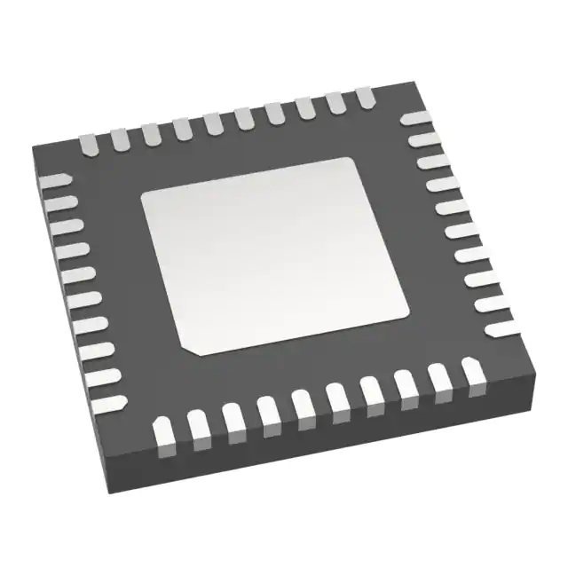
- Part No.:
- ECE1200-I/LD
- Manufacturer:
- Microchip Technology
- Category:
- Specialized
- Package:
- 40-VFQFN Exposed Pad
- Datasheet:
-
 ECE1200-I/LD.pdf
- Description:
- IC INTFACE SPECIALIZED ESPI/LPC
- Quantity:
- Payment:

- Shipping:

Inventory:553
Please send an inquiry. Send us your inquiry, and we will respond immediately.
Product details
Overview
ECE1200-I/LD from Microchip Technology is an eSPI-to-LPC bridge IC designed to enable legacy LPC peripherals in modern Intel chipset platforms supporting eSPI. It provides dual 24 MHz LPC clock outputs, Serial IRQ master interface, CLKRUN# clock control, and ACPI 6.1-compliant S0ix standby support with ≤5 µA standby current. Used in COM Express, POS, and embedded industrial motherboards for backward-compatible I/O expansion.
For engineers reviewing the ECE1200-I/LD datasheet, ECE1200-I/LD pinout, ECE1200-I/LD application, or ECE1200-I/LD equivalent, key selection criteria include eSPI 1.0 compliance, 1.8V/3.3V dual-supply operation, VQFN-40 (LDX) package compatibility, LPC master timing behavior under S0ix, and register-level configurability of base address and decode ranges.
Technical Context
The ECE1200-I/LD implements a hardware bridge translating eSPI Peripheral Channel I/O and Memory cycles into native LPC bus transactions, with strict adherence to Intel LPC Specification 1.1. It supports both Continuous and Quiet modes for Serial IRQ and uses a 48 MHz ring oscillator locked to a 32.768 kHz SUSCLK input to generate precise 24 MHz LPC_CLK[1:0] outputs.
Its power architecture separates VTR_18 (1.8V I/O), VTR_CORE_18 (1.8V core logic), and VTR_33 (3.3V I/O) rails, with LPC_EN enabling VCC-emulated functionality only when main system power is valid. The BOOT_DONE strap determines primary vs. secondary eSPI slave role and selects between SUSPWRDNACK and HOST_RST_ACK on pin 35.
Key Specifications
| Parameter | Value and Actual Design Meaning |
|---|---|
| eSPI Compliance | Intel eSPI Base Specification 1.0 compliant; supports Peripheral and Virtual Wire Channels up to 50 MHz. |
| LPC Compliance | Intel LPC Specification 1.1 compliant; generates 1-byte I/O and memory read/write cycles only. |
| Operating Voltage | 1.8V (VTR_18 & VTR_CORE_18) and 3.3V (VTR_33); requires VTR_33 ≥ VTR_18 during all transitions. |
| LPC Clock Output | Two independent 24 MHz LPC_CLK outputs derived from 48 MHz ring oscillator locked to 32.768 kHz SUSCLK. |
| Standby Current | ≤5 µA in S0ix (Modern Standby) state; enables ultra-low-power platform sleep modes. |
| Temperature Range | Industrial grade: -40°C to +85°C ambient operating range. |
| Package | 40-pin VQFN (LDX), 5×5 mm body with 2.7×2.7 mm exposed pad; RoHS compliant. |
Pinout & Package
40-pin Very Thin Plastic Quad Flat, No Lead (VQFN) package designated LDX per Microchip packaging specification C04-496 Rev A. Body size 5×5 mm, exposed thermal pad 2.7×2.7 mm, pitch 0.4 mm. Requires recommended land pattern with thermal vias tented or filled per drawing C04-2496 Rev A.
| Pin/Terminal | Circuit Role | Design Meaning |
|---|---|---|
| ESPI_ALERT# | eSPI Alert Output | Active-low interrupt to PCH indicating eSPI event requiring host attention; asserted on error or status change. |
| LPC_CLK0 / LPC_CLK1 | LPC Clock Outputs | Two 24 MHz clocks for LPC bus distribution; individually controllable via CLKRUN# and register settings. |
| LAD[3:0] | LPC Multiplexed Bus | 4-bit bidirectional command/address/data bus; carries all LPC I/O and memory transfers to downstream devices. |
| LFRAME# | LPC Frame Strobe | Active-low signal marking start/end of LPC cycle; synchronizes data transfer timing on LAD[3:0]. |
| SER_IRQ | Serial IRQ Interface | Bidirectional pin used with LPC_CLK for daisy-chained interrupt signaling per Serial IRQ v6.0. |
| CLKRUN# | CLKRUN Control | Open-drain bidirectional pin enabling negotiation to gate/un-gate LPC_CLK outputs for power savings. |
| LPC_EN | VCC Emulation Input | Driven by PCH_PWROK; enables VCC-powered behavior on LPC pins only when main system power is stable. |
| BOOT_DONE | eSPI Role Select | Strap pin determining Primary (high) or Secondary (low) eSPI slave mode; selects function of pin 35. |
| SUSPWRDNACK / HOST_RST_ACK | Multiplexed Output | Pin 35 output function determined by BOOT_DONE: SUSPWRDNACK (primary) or HOST_RST_ACK (secondary). |
| RESETI# | Power-On Reset Input | Active-low reset tied to system RSMRST#; must be deasserted after all VTR supplies reach valid levels. |
Key Features
| Feature | Design Value |
|---|---|
| ACPI 6.1 S0ix Support | Enables Modern Standby with sub-5 µA quiescent current, preserving system context while minimizing power draw. |
| ISA Plug-and-Play Compatible Registers | Provides host-programmable base address and configuration registers compatible with legacy ISA PnP enumeration. |
| eSPI-to-LPC Protocol Translation | Transparently converts eSPI Peripheral Channel I/O/Memory cycles into native LPC bus transactions without software intervention. |
| Dual Independent LPC Clocks | Two 24 MHz LPC_CLK outputs allow load balancing and selective clock gating for downstream LPC peripherals. |
| XNOR Board Test Mode | Hardware test mode activated via TEST pin for production validation of pin functionality and internal logic paths. |
Applications
| COM Express Carrier Boards | POS Terminal Motherboards |
|---|---|
Use Scenario: Integrating legacy LPC-based Super I/O (e.g., SCH555x) and SMBus temperature sensors onto COM Express modules with Intel eSPI chipsets. IC Role / Device Role / Timing Role: Acts as protocol bridge enabling LPC peripherals to operate transparently behind eSPI, providing 24 MHz clocks and SER_IRQ routing. Use Value: Eliminates need for discrete level shifters or firmware translation layers while maintaining full ACPI 6.1 S0ix compliance and low standby current. | Use Scenario: Adding secure boot-capable flash controllers and embedded controllers to retail point-of-sale systems using Intel Tiger Lake or Alder Lake PCHs. IC Role / Device Role / Timing Role: Provides LPC master interface for SPI flash and EC communication, with CLKRUN#-controlled clock gating to reduce active power during idle periods. Use Value: Enables certified Windows Modern Standby support in POS systems while retaining compatibility with existing LPC firmware stacks. |
| Industrial Embedded Controllers | Thin Client Reference Designs |
Use Scenario: Supporting legacy LPC watchdog timers, GPIO expanders, and fan controllers in fanless industrial PCs operating across -40°C to +85°C. IC Role / Device Role / Timing Role: Bridges eSPI host to multiple LPC slaves with robust power sequencing (VTR_33/VTR_18/VTR_CORE_18 isolation) and glitch-free RESETI#/LPC_EN timing. Use Value: Ensures reliable boot and runtime operation in harsh environments where voltage sequencing margins are critical. | Use Scenario: Enabling low-cost thin client designs with Intel eSPI chipsets to reuse existing LPC-based audio codecs and debug headers. IC Role / Device Role / Timing Role: Translates eSPI memory-mapped accesses into LPC memory cycles for audio codec configuration and debug trace buffers. Use Value: Reduces BOM cost by avoiding custom ASICs or FPGA-based bridging while meeting Intel Platform Power Requirements v6.0. |
Equivalent & Alternatives
The following parts are listed as comparable options for similar eSPI-to-LPC bridge applications.
| Alternative Part | Technical Difference | Application Difference | Selection Advice |
|---|---|---|---|
| ITE IT8995E | Integrated Super I/O with embedded eSPI-to-LPC bridge; includes UART, GPIO, PWM, and hardware monitor blocks. | Targets designs needing full SIO functionality rather than pure bridge-only use; higher pin count (128-QFP) and larger footprint. | Select IT8995E when consolidating SIO and bridge functions; choose ECE1200-I/LD for minimal-footprint, dedicated bridging with lower standby current. |
| Nuvoton NCT6798D | Super I/O with eSPI slave interface but no native LPC master capability; requires external LPC controller or PCH-native LPC support. | Only suitable where LPC bus is already present on PCH; cannot replace ECE1200-I/LD in eSPI-only platforms lacking native LPC. | Choose NCT6798D for hybrid platforms with both eSPI and LPC; ECE1200-I/LD is required for pure eSPI-to-LPC conversion in new designs. |
Compared with IT8995E and NCT6798D, the ECE1200-I/LD delivers dedicated, low-latency eSPI-to-LPC protocol translation in a compact 5×5 mm VQFN package with industry-leading S0ix current, making it optimal for space-constrained, power-sensitive embedded platforms requiring strict ACPI 6.1 compliance.
Availability
ECE1200-I/LD is available at Aetrix Electronics and suitable for COM Express carrier boards, POS terminal motherboards, industrial embedded controllers, and thin client reference designs requiring stable component supply and long-term lifecycle support.
Supply support for ECE1200-I/LD includes scheduled delivery planning, volume procurement assistance, BOM continuity management, traceable sourcing, and lifecycle availability coordination for OEM customers, industrial embedded developers, connected-device designers, and electronics production programs.
Manufacturer
Microchip Technology Inc. is a leading provider of microcontrollers, analog components, and connectivity solutions, serving automotive, industrial, consumer, and communications markets with high-reliability silicon and development tools.
The ECE1200 product line is designed specifically to bridge the gap between modern Intel eSPI chipsets and legacy LPC peripherals in embedded computing platforms, emphasizing low-power operation, ACPI 6.1 compliance, and seamless integration into space-constrained designs.
FAQ
What is the primary function of the ECE1200-I/LD?
The ECE1200-I/LD is an eSPI-to-LPC bridge IC that translates eSPI Peripheral Channel and Virtual Wire traffic from an Intel chipset into native LPC bus transactions. It enables legacy LPC peripherals-including Super I/O chips, ECs, and SPI flash controllers-to operate in modern eSPI-based platforms while maintaining full ACPI 6.1 S0ix compliance and delivering dual 24 MHz LPC clocks. Its design eliminates the need for software abstraction layers or custom FPGA logic in embedded motherboard designs.
How does the ECE1200-I/LD handle power sequencing and standby states?
The ECE1200-I/LD uses three independent power domains-VTR_33 (3.3V I/O), VTR_18 (1.8V I/O), and VTR_CORE_18 (1.8V core)-with strict sequencing requirements: VTR_33 must be stable before VTR_18/VTR_CORE_18 rise, and RESETI# must be asserted until all VTR rails reach valid levels. In S0ix standby, the device draws ≤5 µA by gating internal clocks and disabling non-essential circuitry while maintaining eSPI alert readiness and SUS_STAT# propagation. LPC_EN must remain high to sustain VCC-emulated functionality during active states.
What are the key timing and clocking features of the ECE1200-I/LD?
The ECE1200-I/LD derives its timing from a 32.768 kHz SUSCLK input to lock a 48 MHz ring oscillator, which then generates two independent 24 MHz LPC_CLK outputs. These clocks support both Continuous and Quiet modes for Serial IRQ and are fully controllable via CLKRUN#. The eSPI interface operates asynchronously at 20–50 MHz, with eSPI_CLK sourced from the PCH. All LPC cycles are strictly 1-byte transfers, and SYNC field handling is limited to Long Wait and Short Wait responses per Intel LPC v1.1.
Can the ECE1200-I/LD operate as both primary and secondary eSPI slave?
Yes-the ECE1200-I/LD's role is determined by the BOOT_DONE strap: when pulled high, it operates as the Primary eSPI Slave with full decode range access and SUSPWRDNACK output on pin 35; when pulled low, it becomes a Secondary eSPI Slave with only one generic I/O and one generic memory decode range, and pin 35 outputs HOST_RST_ACK instead. In secondary mode, handshake responsibilities are shared with the Primary Slave, and certain virtual wires (e.g., HOST_RST_ACK) are presented physically rather than over eSPI.
What package and thermal considerations apply to the ECE1200-I/LD?
The ECE1200-I/LD is housed in a 40-pin VQFN package (LDX) measuring 5×5 mm with a 2.7×2.7 mm exposed thermal pad. Per Microchip drawing C04-2496 Rev A, the PCB land pattern must include thermal vias tented or filled to prevent solder wicking during reflow. The device supports industrial temperature range (-40°C to +85°C) and requires decoupling capacitors on all VTR rails: 100 nF ceramic near each VTR_33 pin, and 100 nF + 1 µF ceramics near VTR_18/VTR_CORE_18 pins. Thermal resistance θJA is 42°C/W typical under JEDEC JESD51-7 conditions.
ECE1200-I/LD Specifications
- Product attributes
- Attribute value
- Manufacturer:
- Microchip Technology
- Series:
- -
- Package/Case:
- 40-VFQFN Exposed Pad
- Packaging:
- Tray
- Product Status:
- Active
- Applications:
- eSPI to LPC Bridge
- Interface:
- LPC
- Voltage - Supply:
- 3.3V
- Supplier Device Package:
- 40-VQFN (5x5)
- Grade:
- -
- Qualification:
- -
- Mounting Type:
- Surface Mount
ECE1200-I/LD FAQ
1.How can I place an order for ECE1200-I/LD through Aetrix?
Please submit a Request for Quotation (RFQ) for ECE1200-I/LD on Aetrix. Our sales agent will provide a competitive quotation and guide you through the order confirmation once you accept the terms.
2.Are the price and stock information for ECE1200-I/LD reliable?
The price and inventory of ECE1200-I/LD are updated periodically and may fluctuate due to market conditions. Stock and pricing data are typically refreshed every 24 hours. Quotation validity for ECE1200-I/LD is usually 5 days.
3.What payment methods are accepted for ECE1200-I/LD?
We accept Wire Transfer, PayPal, Credit Card, Western Union, MoneyGram, and Escrow for ECE1200-I/LD transactions.
Note: Certain payment methods may incur a processing fee.
4.How is shipping managed for ECE1200-I/LD?
ECE1200-I/LD orders can be shipped via leading logistics carriers, including DHL, UPS, FedEx, TNT, or Registered Mail.
Once your ECE1200-I/LD order is processed, you will receive an email with the shipment details and tracking number.
Note: Tracking information may take up to 24 hours to appear. Express delivery typically takes 3–5 business days.
5.How can I obtain technical support or documentation for ECE1200-I/LD?
For technical support, including ECE1200-I/LD datasheets, pinout diagrams, or application guidance, please contact our engineering support team. They can provide detailed documentation and assistance for your ECE1200-I/LD requirements.
6.How does Aetrix verify that ECE1200-I/LD is sourced from the original manufacturer or authorized distributors?
All ECE1200-I/LD products on Aetrix are procured from qualified distributors and authorized channels. Our dedicated quality assurance team conducts strict verification, including traceability checks and, if necessary, third-party testing. This ensures that ECE1200-I/LD meets industry standards.
7.What is the process for return or replacement of ECE1200-I/LD?
All ECE1200-I/LD units undergo pre-shipment inspection (PSI). If there is an issue with ECE1200-I/LD, returns or replacements are accepted under the following conditions:
1.Quantity discrepancies, incorrect items, or visible external defects (such as breakage or corrosion), acknowledged by Aetrix.
2.The issue is reported within 90 days of delivery.
3.The ECE1200-I/LD part is unused and in its original packaging.
Return procedure for ECE1200-I/LD:
1.Submit a request within 90 days.
2.Obtain a Return Material Authorization (RMA) from Aetrix.
ECE1200-I/LD Tags

-
NVT4857UKAZ
NXP Semiconductors

-
TCA8418RTWR
Texas Instruments

-
PCA9546APWR
Texas Instruments

-
MD0100N8-G
Microchip Technology

-
PCA9548APW,118
NXP Semiconductors

-
PCA9540BDP,118
NXP Semiconductors

-
PCA9548APWR
Texas Instruments

-
PCA9546APW,118
NXP Semiconductors

-
PTN3360DBS,518
NXP Semiconductors

-
PCA9546ABS,118
NXP Semiconductors

-
PCA9518PWR
Texas Instruments

-
PCA9545APW,118
NXP Semiconductors
Tech Hub

TTL and CMOS logic families differ in thresholds, loading, output drive, power and timing. This engineering guide compares 74HC and 74HCT, calculates noise margins and checks 3.3 V/5 V compatibility.

A practical engineering guide to 3.3V and 5V logic compatibility, input thresholds, resistor dividers, translator ICs, MOSFET level shifting, I2C pull-ups, timing limits and power-sequencing risks.

The 74HC595 uses push-pull logic outputs, while the TPIC6B595 uses 50 V open-drain DMOS sinks for higher-power loads. This guide compares timing, current limits, 3.3 V interfacing, load wiring, thermal…

The 74HC595 converts serial data into eight stable parallel outputs. This guide covers pin functions, shift and storage timing, OE and MR behavior, drive-current limits, cascading, voltage compatibilit…

A technical comparison of level-sensitive latches and edge-triggered flip-flops, covering timing windows, setup and hold limits, master–slave operation, time borrowing, race-through, HDL inference and…

A D latch stores one bit while Enable controls when data can pass. This reference covers gate-level operation, truth tables, transparency, setup and hold timing, LE versus OE, common ICs and practical …

An SR latch stores one bit through cross-coupled feedback. This engineering reference covers NOR and NAND implementations, truth tables, forbidden-state recovery, gated operation, switch debouncing, fa…

Latch circuits retain one bit through feedback. This technical reference covers SR and D latches, truth tables, transparency, timing limits, latch-versus-flip-flop behavior, applications and common log…

An engineering guide to LED driver operation, constant-current and constant-voltage outputs, linear and switching topologies, dimming, IC selection, calculations, replacement compatibility, and fault c…

Operational amplifier guide covering op amp basics, feedback, ideal vs real op amps, common configurations, buffer circuits, offset, bias current, gain-bandwidth, slew rate, rail-to-rail limits and sel…


