
 My Inquiry
 My Account


STMicroelectronics ECMF02-2HSMX6
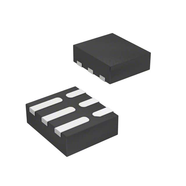
- Part No.:
- ECMF02-2HSMX6
- Manufacturer:
- STMicroelectronics
- Category:
- Common Mode Chokes
- Package:
- 6-UFQFN
- Datasheet:
-
 ECMF02-2HSMX6.pdf
- Description:
- CMC 100MA 2LN SMD ESD
- Quantity:
- Payment:

- Shipping:

Inventory:7,275
Please send an inquiry. Send us your inquiry, and we will respond immediately.
Product details
Overview
ECMF02-2HSMX6 from STMicroelectronics is a 2-line ESD-protected common mode filter for USB3.2 Gen 2 (10 Gbps) differential pairs, featuring –20 dB common mode attenuation at 2.4 GHz and 5 GHz, 7–9 Ω DC serial resistance, ±8 kV IEC 61000-4-2 contact ESD protection, and QFN-6L (1.5 × 1.7 × 0.5 mm) package. It suppresses RFI/EMI in mobile phone antenna regions while preserving signal integrity on high-speed Tx/Rx lines.
For engineers reviewing the ECMF02-2HSMX6 datasheet, ECMF02-2HSMX6 pinout, ECMF02-2HSMX6 application, or ECMF02-2HSMX6 equivalent, key selection criteria include common mode attenuation bandwidth (300 MHz–6 GHz), differential impedance matching (100 Ω), skew control, USB3.2 Gen 2 eye diagram compliance, and µQFN-6L footprint compatibility with high-density PCB layouts.
Technical Context
The device integrates two matched common mode chokes with integrated ESD diodes per line, enabling simultaneous filtering and ±8 kV contact ESD clamping without degrading differential signal fidelity. Its architecture targets full-duplex SuperSpeed USB3.2 lanes operating up to 10 Gbps, with minimal insertion loss (<0.5 dB typical at 5 GHz) and return loss >12 dB across 1–6 GHz.
Designed specifically for host/device-side USB3.2 interface protection, it operates over –55 °C to +125 °C ambient, supports 100 mA DC current per line, and maintains <0.3 ps differential skew to prevent timing violations in high-speed serial links.
Key Specifications
| Parameter | Value and Actual Design Meaning |
|---|---|
| Common mode attenuation | –20 dB at 2.4 & 5 GHz; ensures suppression of cellular/WiFi/GPS band interference in portable devices |
| Differential impedance | 100 Ω nominal; matches USB3.2 differential pair routing for minimal reflection and signal distortion |
| DC serial resistance | 7–9 Ω; limits voltage drop and self-heating under 100 mA operation, preserving power delivery integrity |
| ESD protection level | ±8 kV contact per IEC 61000-4-2; protects transceiver IOs from user-handling ESD events without external TVS |
| Operating temperature | –55 °C to +125 °C; supports deployment in automotive infotainment and industrial USB peripherals |
| Package dimensions | 1.5 × 1.7 × 0.5 mm; enables placement adjacent to USB Type-C connectors in space-constrained mobile PCBs |
Pinout & Package
ECMF02-2HSMX6 uses a µQFN-6L (QFN-6L) package with wettable flanks, measuring 1.5 × 1.7 × 0.5 mm and featuring exposed thermal pad for improved heat dissipation. Pin numbering follows top-view orientation with pin 1 marked by dot.
| Pin/Terminal | Circuit Role | Design Meaning |
|---|---|---|
| 1 | D+ connector | USB3.2 differential pair positive input/output terminal; connects to external connector side |
| 2 | D– connector | USB3.2 differential pair negative input/output terminal; symmetric routing required with Pin 1 |
| 3 | GND | System ground reference; ties internal ESD clamp cathodes and common mode choke center tap |
| 4 | D+ IC | USB3.2 D+ line to SoC/transceiver; must be left floating if unused (not internally connected) |
| 5 | D– IC | USB3.2 D– line to SoC/transceiver; must be left floating if unused (not internally connected) |
| 6 | NC / Floating | No internal connection; electrically isolated; no PCB trace or solder mask opening required |
Key Features
| Feature | Design Value |
|---|---|
| Integrated dual-line common mode choke + ESD diodes | Eliminates need for discrete CMF + TVS stack-up, reducing BOM count by ≥3 components per lane |
| –20 dB CM attenuation at 5 GHz | Prevents desense of 5 GHz WiFi/BT coexistence in smartphones and ultrabooks |
| USB3.2 Gen 2 eye diagram compliance | Validated at 10 Gbps with Type-C connector and equalizer; meets jitter and amplitude mask requirements |
| 0.5 mm profile with wettable flanks | Enables automated optical inspection (AOI) and reflow solder joint quality verification |
| RoHS-compliant ECOPACK® packaging | Meets EU Directive 2011/65/EU and China RoHS II; no lead, cadmium, mercury, hexavalent chromium, PBB, PBDE |
Applications
| Mobile Phone Antenna Coexistence | Notebook USB3.2 Port Protection |
|---|---|
Use Scenario: USB3.2 interface located near LTE/5G or WiFi antennas in slim smartphone chassis. IC Role / Device Role / Timing Role: Common mode noise filter and ESD protector placed between Type-C connector and SoC PHY. Use Value: Reduces radiated emissions in 700 MHz–5 GHz bands by >20 dB, preventing antenna desense and regulatory test failure. | Use Scenario: High-density motherboard layout with multiple USB3.2 ports sharing proximity to DDR4 memory and PCIe traces. IC Role / Device Role / Timing Role: Differential pair EMI suppressor and transient protector on each SuperSpeed lane. Use Value: Maintains <0.3 ps differential skew and >12 dB return loss up to 6 GHz, ensuring Gen 2 link training success. |
| Portable SSD Enclosure Interface | USB-C Docking Station Signal Integrity |
Use Scenario: External NVMe SSD enclosure using USB3.2 Gen 2 for 10 Gbps data transfer. IC Role / Device Role / Timing Role: Front-end common mode filter on both Tx and Rx differential pairs before USB-C receptacle. Use Value: Enables clean eye diagrams at 10 Gbps with reference cable and equalizer, meeting USB-IF compliance test limits. | Use Scenario: Multi-protocol docking station supporting USB3.2, DisplayPort Alt Mode, and PD charging over single Type-C port. IC Role / Device Role / Timing Role: Isolates common mode noise coupling between high-speed data lanes and power delivery circuitry. Use Value: Prevents cross-talk-induced jitter on DP HBR2 (5.4 Gbps) and USB3.2 lanes, verified via eye diagram comparison. |
Equivalent & Alternatives
The following parts are listed as comparable options for similar common mode filter applications.
| Alternative Part | Technical Difference | Application Difference | Selection Advice |
|---|---|---|---|
| TDK MEM2012P50R0 | Single-line, 50 Ω common mode impedance; no integrated ESD diodes; requires external TVS | Limited to USB2.0 or low-speed differential buses; not validated for USB3.2 Gen 2 eye compliance | Select when cost sensitivity outweighs integration benefit and ESD robustness is handled externally |
| ON Semiconductor NUF2221MUTAG | 2-line, 100 Ω impedance, but only –12 dB CM attenuation at 5 GHz; ±15 kV air discharge ESD rating | Lower RF filtering performance; suitable for less demanding EMI environments where higher ESD margin is critical | Choose when system-level ESD testing exceeds ±8 kV contact but USB3.2 radiation limits are relaxed |
Compared with TDK MEM2012P50R0 and ON Semi NUF2221MUTAG, ECMF02-2HSMX6 uniquely delivers Gen 2–compliant eye diagrams, –20 dB CM attenuation at 5 GHz, and monolithic ESD+CMF integration-enabling smaller footprints and eliminating discrete TVS placement and routing complexity.
Availability
ECMF02-2HSMX6 is available at Aetrix Electronics and suitable for mobile phone antenna coexistence, notebook USB3.2 port protection, and portable SSD enclosure interface requiring stable component supply and full USB-IF compliance support.
Supply support for ECMF02-2HSMX6 includes scheduled delivery planning, volume procurement assistance, BOM continuity management, traceable sourcing, and lifecycle availability coordination for OEM customers, industrial embedded developers, connected-device designers, and electronics production programs.
Manufacturer
STMicroelectronics is a global semiconductor leader headquartered in Geneva, Switzerland, designing and manufacturing microcontrollers, analog ICs, power management, sensors, and discrete components for industrial, automotive, and consumer markets.
The ECMF series targets high-speed interface protection, with ECMF02-2HSMX6 developed specifically to solve EMI/ESD challenges in USB3.2 Gen 2 and DisplayPort HBR2 systems where board space and signal integrity are critical constraints.
FAQ
What is the maximum data rate supported by ECMF02-2HSMX6?
ECMF02-2HSMX6 is validated for USB3.2 Gen 2 operation at 10 Gbps, with eye diagram compliance confirmed in Figures 16–17 of DS9863 Rev 4. Its differential insertion loss remains below 0.5 dB up to 6 GHz, supporting full Gen 2 bandwidth without equalization degradation.
Can Pin 4 (D+ IC) and Pin 5 (D– IC) be left unconnected?
Yes - Pins 4 and 5 are designated "To be left floating" per the functional diagram and datasheet. They are not internally connected and must remain un-routed on PCB to avoid parasitic coupling or unintended grounding paths that degrade common mode rejection.
Does ECMF02-2HSMX6 require external bias or control signals?
No - ECMF02-2HSMX6 is a passive, fully integrated filter with no external bias, enable pins, or configuration interfaces. It operates transparently in-series with the differential pair and requires only proper GND connection (Pin 3) and correct PCB layout per ST's footprint recommendations.
How does ECMF02-2HSMX6 compare to discrete CMF + TVS solutions in terms of board area?
ECMF02-2HSMX6 occupies 2.55 mm² (1.5 × 1.7 mm), replacing ~3 discrete components (two CM chokes + one dual-channel TVS) requiring ≥6 mm² total area including spacing. This 58% reduction enables placement directly at USB-C connector pads, minimizing stub length and improving high-frequency EMI performance.
ECMF02-2HSMX6 Specifications
- Product attributes
- Attribute value
- Manufacturer:
- STMicroelectronics
- Package/Case:
- 6-UFQFN
- Filter Type:
- Signal Line
- Number of Lines:
- 2
- Impedance @ Frequency:
- -
- Current Rating (Max):
- -
- DC Resistance (DCR) (Max):
- 100mA
- Voltage Rating - DC:
- 9Ohm
- Voltage Rating - AC:
- -
- Operating Temperature:
- -
- Ratings:
- -40°C ~ 85°C
- Approval Agency:
- -
- Features:
- -
- Mounting Type:
- TVS Diode ESD Protection
- Size / Dimension:
- -
- Height (Max):
- -
ECMF02-2HSMX6 FAQ
1.How can I place an order for ECMF02-2HSMX6 through Aetrix?
Please submit a Request for Quotation (RFQ) for ECMF02-2HSMX6 on Aetrix. Our sales agent will provide a competitive quotation and guide you through the order confirmation once you accept the terms.
2.Are the price and stock information for ECMF02-2HSMX6 reliable?
The price and inventory of ECMF02-2HSMX6 are updated periodically and may fluctuate due to market conditions. Stock and pricing data are typically refreshed every 24 hours. Quotation validity for ECMF02-2HSMX6 is usually 5 days.
3.What payment methods are accepted for ECMF02-2HSMX6?
We accept Wire Transfer, PayPal, Credit Card, Western Union, MoneyGram, and Escrow for ECMF02-2HSMX6 transactions.
Note: Certain payment methods may incur a processing fee.
4.How is shipping managed for ECMF02-2HSMX6?
ECMF02-2HSMX6 orders can be shipped via leading logistics carriers, including DHL, UPS, FedEx, TNT, or Registered Mail.
Once your ECMF02-2HSMX6 order is processed, you will receive an email with the shipment details and tracking number.
Note: Tracking information may take up to 24 hours to appear. Express delivery typically takes 3–5 business days.
5.How can I obtain technical support or documentation for ECMF02-2HSMX6?
For technical support, including ECMF02-2HSMX6 datasheets, pinout diagrams, or application guidance, please contact our engineering support team. They can provide detailed documentation and assistance for your ECMF02-2HSMX6 requirements.
6.How does Aetrix verify that ECMF02-2HSMX6 is sourced from the original manufacturer or authorized distributors?
All ECMF02-2HSMX6 products on Aetrix are procured from qualified distributors and authorized channels. Our dedicated quality assurance team conducts strict verification, including traceability checks and, if necessary, third-party testing. This ensures that ECMF02-2HSMX6 meets industry standards.
7.What is the process for return or replacement of ECMF02-2HSMX6?
All ECMF02-2HSMX6 units undergo pre-shipment inspection (PSI). If there is an issue with ECMF02-2HSMX6, returns or replacements are accepted under the following conditions:
1.Quantity discrepancies, incorrect items, or visible external defects (such as breakage or corrosion), acknowledged by Aetrix.
2.The issue is reported within 90 days of delivery.
3.The ECMF02-2HSMX6 part is unused and in its original packaging.
Return procedure for ECMF02-2HSMX6:
1.Submit a request within 90 days.
2.Obtain a Return Material Authorization (RMA) from Aetrix.
ECMF02-2HSMX6 Tags
-4-Lead.jpg)
-
DLM0NSN900HY2D
Murata Electronics
-
DLM0NSM900HY2D
Murata Electronics

-
DLM0QSN900HY2D
Murata Electronics
-
TCM0605M-900-2P-T201
TDK Corporation
-
LCFE121002A900TG
Littelfuse Inc.
-
DLM11SN900HZ2L
Murata Electronics
-
ACM2012H-381-2P-T05
TDK Corporation
-
SRF2012-900YA
Bourns Inc.
-
ACM2012-900-2P-T002
TDK Corporation
-
ACM2012-361-2P-T002
TDK Corporation
-
ACM2012-121-2P-T002
TDK Corporation
-
ACM2012D-900-2P-T00
TDK Corporation
Tech Hub

A practical engineering and sourcing framework covering lifecycle verification, lifetime-buy calculations, replacement qualification, supplier checks and counterfeit-risk controls.

TTL and CMOS logic families differ in thresholds, loading, output drive, power and timing. This engineering guide compares 74HC and 74HCT, calculates noise margins and checks 3.3 V/5 V compatibility.

A practical engineering guide to 3.3V and 5V logic compatibility, input thresholds, resistor dividers, translator ICs, MOSFET level shifting, I2C pull-ups, timing limits and power-sequencing risks.

The 74HC595 uses push-pull logic outputs, while the TPIC6B595 uses 50 V open-drain DMOS sinks for higher-power loads. This guide compares timing, current limits, 3.3 V interfacing, load wiring, thermal…

The 74HC595 converts serial data into eight stable parallel outputs. This guide covers pin functions, shift and storage timing, OE and MR behavior, drive-current limits, cascading, voltage compatibilit…

A technical comparison of level-sensitive latches and edge-triggered flip-flops, covering timing windows, setup and hold limits, master–slave operation, time borrowing, race-through, HDL inference and…

A D latch stores one bit while Enable controls when data can pass. This reference covers gate-level operation, truth tables, transparency, setup and hold timing, LE versus OE, common ICs and practical …

An SR latch stores one bit through cross-coupled feedback. This engineering reference covers NOR and NAND implementations, truth tables, forbidden-state recovery, gated operation, switch debouncing, fa…

Latch circuits retain one bit through feedback. This technical reference covers SR and D latches, truth tables, transparency, timing limits, latch-versus-flip-flop behavior, applications and common log…

An engineering guide to LED driver operation, constant-current and constant-voltage outputs, linear and switching topologies, dimming, IC selection, calculations, replacement compatibility, and fault c…


