
 My Inquiry
 My Account


STMicroelectronics ECMF04-4HSWM10
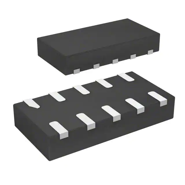
- Part No.:
- ECMF04-4HSWM10
- Manufacturer:
- STMicroelectronics
- Category:
- Common Mode Chokes
- Package:
- 10-UFDFN
- Datasheet:
-
 ECMF04-4HSWM10.pdf
- Description:
- CMC 100MA 4LN SMD ESD
- Quantity:
- Payment:

- Shipping:

Inventory:11,779
Please send an inquiry. Send us your inquiry, and we will respond immediately.
Product details
Overview
ECMF04-4HSWM10 from STMicroelectronics is a high-speed common mode filter with integrated ESD protection for two differential lanes (D1+, D1−, D2+, D2−), designed for HDMI Full HD, MIPI D-PHY 2.5 Gbps, USB3.2 Gen 1 (5.0 Gbps), and DisplayPort interfaces. It delivers −28 dB common mode attenuation at 2.4 GHz, 4.2 GHz differential bandwidth, and ±8 kV contact/±15 kV air ESD robustness per IEC 61000-4-2 Level 4.
For engineers reviewing the ECMF04-4HSWM10 datasheet, ECMF04-4HSWM10 pinout, ECMF04-4HSWM10 application in high-speed serial buses, or ECMF04-4HSWM10 equivalent for EMI filtering and ESD co-protection, this device provides verified differential signal integrity preservation while suppressing common mode noise across WLAN, LTE, GSM, and GPS bands - critical for compact mobile and portable designs.
Technical Context
This device integrates four-channel ESD protection (two fully differential lanes) with a monolithic common mode choke structure optimized for impedance matching to 100 Ω differential and 50 Ω common mode lines. Its architecture enables simultaneous suppression of common mode noise above 100 MHz while preserving >4.2 GHz differential bandwidth - validated via HDMI 2.0 (5.94 Gbps), USB3.2 Gen 1 (5.0 Gbps), and MIPI D-PHY (2.5 Gbps) eye diagram testing.
It operates over −55 °C to +125 °C ambient, features 5 Ω typical DC series resistance per line, 4.5–5.5 V breakdown voltage (IR = 1 mA), and <100 nA leakage at 3 V per line - ensuring minimal insertion loss and signal distortion in high-speed data paths without active biasing or external components.
Key Specifications
| Parameter | Value and Actual Design Meaning |
|---|---|
| Differential bandwidth | 4.2 GHz (−3 dB cutoff): preserves signal integrity up to HDMI 2.0 / USB3.2 Gen 1 data rates |
| Common mode attenuation | −28 dB @ 2.4 GHz, −16 dB @ 5.0 GHz: suppresses WLAN interference in mobile RF front-ends |
| ESD protection level | ±8 kV contact / ±15 kV air (IEC 61000-4-2 Level 4): protects interface ICs from system-level ESD events |
| DC series resistance | 5 Ω max per line: limits insertion loss and voltage drop in high-speed differential pairs |
| Breakdown voltage | 4.5–5.5 V (IR = 1 mA): ensures reliable clamping before downstream PHY damage |
| Operating temperature | −55 °C to +125 °C: supports automotive-grade thermal cycling in portable electronics |
Pinout & Package
Package: µQFN-10L (2.6 × 1.35 × 0.55 mm max height), RoHS-compliant ECOPACK® with exposed thermal pad (GND-connected).
| Pin/Terminal | Circuit Role | Design Meaning |
|---|---|---|
| 1 | D1+ to connector | High-speed differential input from external port (e.g., HDMI receptacle) |
| 2 | D1− to connector | Complementary input for first differential lane; matched length routing required |
| 3 | GND | Primary ground reference for ESD discharge path and common mode choke return |
| 4 | D2+ to connector | Second differential lane input from external interface |
| 5 | D2− to connector | Complementary input for second differential lane |
| 6 | D2− to IC | Output to SoC/PHY IC; maintains signal polarity and impedance continuity |
| 7 | D2+ to IC | Matched output for second lane; routed with controlled 100 Ω differential impedance |
| 8 | GND | Secondary ground terminal; connects to PCB ground plane under package |
| 9 | D1− to IC | First lane output to host IC; low-inductance path minimizes common mode conversion |
| 10 | D1+ to IC | First lane output; pin 10 aligns with dot marking for orientation verification |
Key Features
| Feature | Design Value |
|---|---|
| Integrated dual-lane common mode filtering | Single-component solution for two independent high-speed differential buses (e.g., HDMI + MIPI or dual USB lanes) |
| Monolithic ESD + filtering co-design | Eliminates need for discrete TVS diodes and separate CM chokes - reduces BOM count and PCB area by >40% |
| Ultra-thin profile (0.55 mm max) | Enables placement under narrow bezels or beneath display flex cables in smartphones and ultra-thin notebooks |
| Low parasitic design | Minimizes self-resonance and impedance discontinuity - validated by preserved eye opening in 5.94 Gbps HDMI tests |
| ECOPACK® RoHS-compliant packaging | Meets global environmental regulations without compromising thermal or mechanical reliability |
Applications
| Mobile Phone Front-End Filtering | Notebook High-Speed Port Protection |
|---|---|
Use Scenario: Suppressing common mode noise coupling from cellular/Wi-Fi antennas into HDMI or MIPI D-PHY traces on shared PCB layers. IC Role / Device Role / Timing Role: Common mode choke + ESD protector placed between display/camera module connectors and baseband/AP SoC. Use Value: Prevents antenna desense and video corruption by attenuating −28 dB at 2.4 GHz while maintaining HDMI 2.0 eye margin. | Use Scenario: Protecting USB3.2 Gen 1 Type-C ports from ESD and RFI during hot-plug events in thin-profile laptops. IC Role / Device Role / Timing Role: Dual-lane ESD filter bridging external port and USB controller PHY, with GND pins tied to chassis ground. Use Value: Enables compliance with IEC 61000-4-2 Level 4 without degrading 5.0 Gbps signal integrity - confirmed by eye diagram testing. |
| Portable Navigation Device (PND) Display Interface | Tablet MIPI DSI Link Stabilization |
Use Scenario: Filtering common mode noise on LVDS or DisplayPort signals driving high-resolution LCDs in GPS-enabled handheld units. IC Role / Device Role / Timing Role: Differential EMI filter placed inline between display controller and panel connector, with direct GND tie to metal shield. Use Value: Reduces radiated emissions by >10 dB in 30–1000 MHz range while supporting full 4.2 GHz bandwidth for 1080p60 video. | Use Scenario: Stabilizing MIPI D-PHY 2.5 Gbps DSI links in tablets where flex cable routing induces common mode currents. IC Role / Device Role / Timing Role: Common mode suppression element between application processor DSI outputs and display timing controller inputs. Use Value: Restores eye height and jitter margin in long-reference-channel MIPI tests - validated in DS10228 Figure 12–13. |
Equivalent & Alternatives
The following parts are listed as comparable options for similar common mode filtering with ESD protection applications.
| Alternative Part | Technical Difference | Application Difference | Selection Advice |
|---|---|---|---|
| TPD4E05U06DQAR | Quad-channel ESD array only (no integrated common mode choke); 0.5 pF line capacitance vs. ECMF04's 0.25 pF typical | Lacks differential bandwidth optimization; requires external CM choke for HDMI/MIPI noise suppression | Select when ESD-only protection suffices and board space allows discrete choke integration |
| CM1422-04SO | 4-line common mode filter without ESD diodes; requires external TVS for IEC 61000-4-2 compliance | Higher total solution size; no integrated clamping - adds routing complexity and potential impedance mismatch | Choose for cost-sensitive industrial designs where ESD threat level is lower than consumer mobile |
Compared with TPD4E05U06DQAR and CM1422-04SO, ECMF04-4HSWM10 uniquely combines broadband differential signal fidelity, high-frequency common mode rejection, and certified Level 4 ESD protection in one µQFN-10L package - eliminating design trade-offs between noise suppression, surge robustness, and PCB real estate in space-constrained portable systems.
Availability
ECMF04-4HSWM10 is available at Aetrix Electronics and suitable for mobile phone front-end filtering, notebook high-speed port protection, and portable navigation device (PND) display interface applications requiring stable component supply and guaranteed long-term lifecycle support.
Supply support for ECMF04-4HSWM10 includes scheduled delivery planning, volume procurement assistance, BOM continuity management, traceable sourcing, and lifecycle availability coordination for OEM customers, industrial embedded developers, connected-device designers, and electronics production programs.
Manufacturer
STMicroelectronics is a global semiconductor leader headquartered in Geneva, Switzerland, designing and manufacturing analog, microcontroller, power, and sensor solutions for automotive, industrial, and consumer markets.
This device belongs to ST's ECMF series of integrated EMI filters - engineered specifically for high-speed serial interface protection in compact, battery-powered devices where board space, thermal profile, and electromagnetic compatibility are critical constraints.
FAQ
What is the maximum data rate supported by ECMF04-4HSWM10?
The device supports differential signaling up to 5.94 Gbps, validated with HDMI 2.0 eye diagrams and USB3.2 Gen 1 (5.0 Gbps) compliance testing. Its 4.2 GHz −3 dB differential bandwidth ensures minimal intersymbol interference and jitter accumulation at these rates, provided PCB layout follows 100 Ω differential impedance control and matched trace lengths.
Can ECMF04-4HSWM10 be used for single-ended interfaces like USB 2.0?
No - it is designed exclusively for differential signaling standards including HDMI, MIPI D-PHY, USB3.2 Gen 1, and DisplayPort. Its internal common mode choke architecture requires balanced differential pairs; applying it to single-ended lines would cause severe signal degradation and violate its specified electrical characteristics.
How does the GND pin configuration affect ESD performance?
Pins 3 and 8 provide dual low-inductance GND connections that form the primary discharge path for ESD events. Both must be soldered to a solid, low-impedance PCB ground plane - ideally with multiple vias to inner ground layers - to achieve the rated ±8 kV contact discharge performance. Floating or undersized GND pads degrade clamping response and increase risk of downstream IC damage.
Is reflow profile adjustment needed for µQFN-10L mounting?
Yes - ST specifies a peak reflow temperature of 240–245 °C with ≤60 seconds above 210 °C, using halide-free, fine-particle (20–38 μm) solder paste. Exceeding 245 °C or prolonged dwell time risks delamination of the ultra-thin package or damage to internal bond wires, directly impacting ESD robustness and high-frequency performance.
ECMF04-4HSWM10 Specifications
- Product attributes
- Attribute value
- Manufacturer:
- STMicroelectronics
- Package/Case:
- 10-UFDFN
- Filter Type:
- Signal Line
- Number of Lines:
- 4
- Impedance @ Frequency:
- -
- Current Rating (Max):
- -
- DC Resistance (DCR) (Max):
- 100mA
- Voltage Rating - DC:
- 5Ohm (Typ)
- Voltage Rating - AC:
- -
- Operating Temperature:
- -
- Ratings:
- -40°C ~ 85°C
- Approval Agency:
- -
- Features:
- -
- Mounting Type:
- TVS Diode ESD Protection
- Size / Dimension:
- -
- Height (Max):
- -
ECMF04-4HSWM10 FAQ
1.How can I place an order for ECMF04-4HSWM10 through Aetrix?
Please submit a Request for Quotation (RFQ) for ECMF04-4HSWM10 on Aetrix. Our sales agent will provide a competitive quotation and guide you through the order confirmation once you accept the terms.
2.Are the price and stock information for ECMF04-4HSWM10 reliable?
The price and inventory of ECMF04-4HSWM10 are updated periodically and may fluctuate due to market conditions. Stock and pricing data are typically refreshed every 24 hours. Quotation validity for ECMF04-4HSWM10 is usually 5 days.
3.What payment methods are accepted for ECMF04-4HSWM10?
We accept Wire Transfer, PayPal, Credit Card, Western Union, MoneyGram, and Escrow for ECMF04-4HSWM10 transactions.
Note: Certain payment methods may incur a processing fee.
4.How is shipping managed for ECMF04-4HSWM10?
ECMF04-4HSWM10 orders can be shipped via leading logistics carriers, including DHL, UPS, FedEx, TNT, or Registered Mail.
Once your ECMF04-4HSWM10 order is processed, you will receive an email with the shipment details and tracking number.
Note: Tracking information may take up to 24 hours to appear. Express delivery typically takes 3–5 business days.
5.How can I obtain technical support or documentation for ECMF04-4HSWM10?
For technical support, including ECMF04-4HSWM10 datasheets, pinout diagrams, or application guidance, please contact our engineering support team. They can provide detailed documentation and assistance for your ECMF04-4HSWM10 requirements.
6.How does Aetrix verify that ECMF04-4HSWM10 is sourced from the original manufacturer or authorized distributors?
All ECMF04-4HSWM10 products on Aetrix are procured from qualified distributors and authorized channels. Our dedicated quality assurance team conducts strict verification, including traceability checks and, if necessary, third-party testing. This ensures that ECMF04-4HSWM10 meets industry standards.
7.What is the process for return or replacement of ECMF04-4HSWM10?
All ECMF04-4HSWM10 units undergo pre-shipment inspection (PSI). If there is an issue with ECMF04-4HSWM10, returns or replacements are accepted under the following conditions:
1.Quantity discrepancies, incorrect items, or visible external defects (such as breakage or corrosion), acknowledged by Aetrix.
2.The issue is reported within 90 days of delivery.
3.The ECMF04-4HSWM10 part is unused and in its original packaging.
Return procedure for ECMF04-4HSWM10:
1.Submit a request within 90 days.
2.Obtain a Return Material Authorization (RMA) from Aetrix.
ECMF04-4HSWM10 Tags
-4-Lead.jpg)
-
DLM0NSN900HY2D
Murata Electronics
-
DLM0NSM900HY2D
Murata Electronics

-
DLM0QSN900HY2D
Murata Electronics
-
TCM0605M-900-2P-T201
TDK Corporation
-
LCFE121002A900TG
Littelfuse Inc.
-
DLM11SN900HZ2L
Murata Electronics
-
ACM2012H-381-2P-T05
TDK Corporation
-
SRF2012-900YA
Bourns Inc.
-
ACM2012-900-2P-T002
TDK Corporation
-
ACM2012-361-2P-T002
TDK Corporation
-
ACM2012-121-2P-T002
TDK Corporation
-
ACM2012D-900-2P-T00
TDK Corporation
Tech Hub

A practical engineering and sourcing framework covering lifecycle verification, lifetime-buy calculations, replacement qualification, supplier checks and counterfeit-risk controls.

TTL and CMOS logic families differ in thresholds, loading, output drive, power and timing. This engineering guide compares 74HC and 74HCT, calculates noise margins and checks 3.3 V/5 V compatibility.

A practical engineering guide to 3.3V and 5V logic compatibility, input thresholds, resistor dividers, translator ICs, MOSFET level shifting, I2C pull-ups, timing limits and power-sequencing risks.

The 74HC595 uses push-pull logic outputs, while the TPIC6B595 uses 50 V open-drain DMOS sinks for higher-power loads. This guide compares timing, current limits, 3.3 V interfacing, load wiring, thermal…

The 74HC595 converts serial data into eight stable parallel outputs. This guide covers pin functions, shift and storage timing, OE and MR behavior, drive-current limits, cascading, voltage compatibilit…

A technical comparison of level-sensitive latches and edge-triggered flip-flops, covering timing windows, setup and hold limits, master–slave operation, time borrowing, race-through, HDL inference and…

A D latch stores one bit while Enable controls when data can pass. This reference covers gate-level operation, truth tables, transparency, setup and hold timing, LE versus OE, common ICs and practical …

An SR latch stores one bit through cross-coupled feedback. This engineering reference covers NOR and NAND implementations, truth tables, forbidden-state recovery, gated operation, switch debouncing, fa…

Latch circuits retain one bit through feedback. This technical reference covers SR and D latches, truth tables, transparency, timing limits, latch-versus-flip-flop behavior, applications and common log…

An engineering guide to LED driver operation, constant-current and constant-voltage outputs, linear and switching topologies, dimming, IC selection, calculations, replacement compatibility, and fault c…


