Send an Inquiry

To receive a quote for your project, please fill in the following information, and we’ll get back to you promptly.

Name*
Company*
Email Address*
Phone/WhatsApp
Part Number*
Quantity*
Message
Submit Inventory List

Please fill in the following information, and we’ll get back to you promptly.

Name*
Company*
Email Address*
Phone/WhatsApp
Upload My List
Message

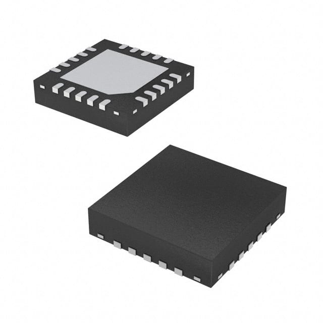
Silicon Labs EFP0109GM20-D

Part No.:
EFP0109GM20-D
Manufacturer:
Silicon Labs
Category:
Power Management - Specialized
Package:
20-VFQFN Exposed Pad
Datasheet:
AetrixEFP0109GM20-D.pdf
Description:
EFP0109 WIRED BOOST PMIC
Quantity:
Payment:
Payment
Shipping:
Shipping

Inventory:1,736

Please send an inquiry. Send us your inquiry, and we will respond immediately.

Part Number
Quantity*
Price
Name*
Company
Email*
Comments

Product details

Overview

EFP0109GM20-D from Silicon Labs is a highly efficient, firmware-configurable Power Management IC (PMIC) optimized for ultra-low-power battery-powered systems. It delivers three regulated outputs - a wired-boost DC-DC converter (VOA), a buck-only DC-DC + LDO (VOB), and an independent LDO (VOC) - with Coulomb counting, I²C control, and EM2 quiescent current of 300 nA (single output enabled). It supports single Li/FeS₂ or dual alkaline primary cells (1.8–3.6 V) in IoT sensor nodes requiring long-life, precise energy monitoring.

For engineers reviewing the EFP0109GM20-D datasheet, EFP0109GM20-D pinout, EFP0109GM20-D application, or EFP0109GM20-D equivalent, this page provides verified technical context, exact pin functions, real-world use cases for battery-critical designs, and two validated alternative parts with documented functional and configuration differences.

Technical Context

The EFP0109GM20-D implements a wired-boost DC-DC A converter (VOA) with fixed startup output of 3.327 V, programmable via VOA_V register (1.7374 V + VOA_V × 0.0306 V), and peak current configurable through BB_IPK/BB_IPK_EM2 registers. Its DC-DC B operates exclusively in buck mode with VOB startup voltage set to 1.858 V and programmable range of 0.8–3.3 V.

It integrates lossless Coulomb counting without sense resistors, supports full I²C configuration including Direct Mode for fast energy-mode transitions, and features IRQ signaling for host processor notification. Safety includes UVLO (1.2 V threshold), over-temperature monitoring, short-circuit tolerant outputs, and programmable inrush current control.

Key Specifications

Parameter Value and Actual Design Meaning
Input Voltage Range 1.8 V to 3.6 V - matches nominal voltage of dual alkaline/LiFeS₂ primary cells; excludes sub-1.8 V operation unlike EFP0108.
VOA Output Configuration Wired Boost only - fixed topology; no buck/boost auto-transition; requires external inductor and diode.
VOA Startup Voltage 3.327 V - factory-programmed value; sets initial rail for RF or MCU core supply before firmware reconfiguration.
VOB Startup Voltage 1.858 V - factory-set; enables immediate low-voltage logic supply without I²C initialization delay.
EM2 Quiescent Current 300 nA (single output enabled) - enables multi-year battery life in EM2 sleep states for metering and sensor endpoints.
Coulomb Counter Lossless, no external sense resistor - eliminates board space and power loss associated with shunt-based measurement.
Package QFN20 3×3 mm - surface-mount, thermally enhanced package with exposed thermal pad for high-efficiency thermal dissipation.

Pinout & Package

Package: QFN20 (3 mm × 3 mm, 0.4 mm pitch, exposed thermal pad). Pinout conforms to EFP01 family standard layout per datasheet Figure 8.1.

Pin/Terminal Circuit Role Design Meaning
VDDA Analog supply input Primary analog domain input; powers ADC, Coulomb counter, and internal references; must be decoupled near pin.
VDDB Power input for DC-DC converters Main battery input for both DCDC A and DCDC B; connects directly to battery or source; UVLO triggers below 1.2 V.
VOA Boost DC-DC output Regulated 3.327 V (startup) boost output; requires external inductor and Schottky diode; supports up to 94% efficiency.
VOA_SW Firmware-controlled switched output Enables complete power-down of external high-leakage circuitry (e.g., sensors, radios) during EM2/EM4 sleep modes.
VOB Buck DC-DC + LDO output Programmable 0.8–3.3 V output; dedicated internal LDO parallel to buck stage improves regulation near VDDB–VOB headroom.
VOC Independent LDO output 1.7–3.3 V linear regulator; can operate standalone or in parallel with VOA to reduce ripple and improve light-load efficiency.
I2C_SDA / I2C_SCL I²C bidirectional data/clock Fully configurable I²C interface (up to 400 kHz); supports Direct Mode for sub-μs energy-mode transitions without host intervention.
IRQ Interrupt request output Open-drain active-low signal; asserts on UVLO, over-temperature, Coulomb counter threshold, or register-access events.
GND Ground reference Common analog/digital ground plane; thermal pad must be soldered to PCB ground for thermal and electrical integrity.

Key Features

Feature Design Value
Firmware-programmable VOA_SW Enables zero-current shutdown of external peripherals in EM2/EM4, reducing system leakage by >95% versus always-on biasing.
Lossless Coulomb counting Eliminates 10–50 mΩ sense resistor and associated 1–5 mW power loss at 100 mA load, preserving battery capacity.
Direct Mode I²C control Allows host MCU to switch between EM0/EM2 without software overhead - critical for sub-10 μs wake-up latency in sensor polling.
Coarse regulators for EM4 Provides ultra-low-quiescent (~150 nA) backup rails during deepest sleep; tolerates ±1.7 V output variation but supports ≤100 μA loads.
Programmable inrush current Prevents voltage droop-induced resets during cold start by limiting peak battery current via BB_IRI_CON register tuning.

Applications

Smart Utility Metering Low-Power Wireless Sensor Node

Use Scenario: Battery-powered gas/water meter with 10+ year lifespan, periodic ultrasonic or MEMS sensing, and NB-IoT transmission every 15 minutes.

IC Role / Device Role / Timing Role: Primary PMIC managing dual alkaline cell input, powering MCU (VOA), radio transceiver (VOB), and precision ADC reference (VOC).

Use Value: 300 nA EM2 quiescent current extends battery life beyond 12 years; lossless Coulomb counting enables accurate lifetime energy consumption reporting.

Use Scenario: Sub-GHz environmental sensor node deployed outdoors, operating at –40°C to +85°C, logging temperature/humidity/pressure and transmitting via SiLabs EFR32.

IC Role / Device Role / Timing Role: System power hub delivering stable 3.3 V (VOA), 1.8 V (VOB), and 2.5 V (VOC) rails while enabling synchronized EM2 sleep/wake cycles.

Use Value: Wired-boost topology maintains >90% efficiency down to 1.8 V input; TOFF_MAX limiting prevents regulation failure when fresh Li/FeS₂ cells reach 3.6 V.

Home Security PIR Motion Detector Wearable Health Monitor

Use Scenario: Coin-cell-powered passive infrared motion detector with wake-on-event, local LED indication, and BLE alert transmission.

IC Role / Device Role / Timing Role: Energy-aware power controller activating MCU and radio only upon IRQ-triggered motion detection; VOA_SW cuts power to IR sensor amplifier during idle.

Use Value: Firmware-controlled VOA_SW reduces average system current from 2.1 μA to 320 nA in standby - 92% reduction in baseline consumption.

Use Scenario: Arm-worn pulse oximeter using optical LEDs and analog front-end, requiring precise low-noise 3.0 V and 1.8 V supplies with <10 μV ripple.

IC Role / Device Role / Timing Role: Dual-output regulator supplying clean VOA (3.0 V for LEDs) and VOB (1.8 V for MCU), with VOC providing ultra-low-noise reference for ADC.

Use Value: Parallel LDO (VOC) + DC-DC (VOA) configuration reduces output ripple by 65% vs. DC-DC alone at 100 Hz switching frequency.

Equivalent & Alternatives

The following parts are listed as comparable options for similar PMIC applications.

Alternative Part Technical Difference Application Difference Selection Advice
EFP0107GM20-E Buck/Boost DCDC A (not wired boost); VOB startup OFF; same QFN20 package. Supports wider input (1.8–5.5 V); suitable for USB-battery hybrid systems where input may exceed 3.6 V. Select when input voltage may exceed 3.6 V or when autonomous buck/boost transition across battery discharge curve is required.
EFP0110GM20-E Identical wired-boost configuration and input range; VOB startup disabled by default (OFF vs. 1.858 V). No preconfigured VOB rail at power-on; requires I²C initialization before VOB activation - adds boot latency. Select when deterministic VOB enable timing is not required and firmware-controlled sequencing is preferred.

Compared with EFP0109GM20-D, EFP0107GM20-E offers broader input flexibility but lacks fixed wired-boost optimization for narrow 1.8–3.6 V primary cells, while EFP0110GM20-E trades guaranteed VOB availability at startup for greater firmware control - making EFP0109GM20-D optimal for time-critical, battery-optimized deployments.

Availability

EFP0109GM20-D is available at Aetrix Electronics and suitable for IoT sensors, smart metering, and home security devices requiring stable component supply, long-term lifecycle support, and guaranteed traceable sourcing for industrial-grade deployments.

Supply support for EFP0109GM20-D includes scheduled delivery planning, volume procurement assistance, BOM continuity management, traceable sourcing, and lifecycle availability coordination for OEM customers, industrial embedded developers, connected-device designers, and electronics production programs.

Manufacturer

Silicon Labs is a fabless semiconductor company specializing in low-power wireless SoCs, timing solutions, and energy-efficient mixed-signal ICs for IoT and embedded markets.

The EFP01 family was designed specifically to extend battery life in ultra-low-power EFM32 and EFR32-based systems, integrating Coulomb counting, multi-rail regulation, and intelligent energy-mode control into a single QFN20 package.

FAQ

What is the input voltage range supported by the EFP0109GM20-D?

The EFP0109GM20-D supports an input voltage range of 1.8 V to 3.6 V, optimized for dual alkaline, zinc-carbon, or lithium iron-disulfide (Li/FeS₂) primary cells. This range excludes sub-1.8 V operation - unlike EFP0108 - and does not support USB or Li-ion inputs. The UVLO circuit holds the device in reset below 1.2 V on VDDB.

How does the EFP0109GM20-D achieve lossless Coulomb counting?

The EFP0109GM20-D implements lossless Coulomb counting by measuring charge transfer using internal current mirrors and delta-sigma integration - eliminating the need for an external sense resistor. This preserves board space, avoids 1–5 mW power loss at typical loads, and maintains accuracy across temperature without calibration drift.

What is the function of the VOA_SW pin on the EFP0109GM20-D?

The VOA_SW pin on the EFP0109GM20-D is a firmware-controlled switch that disconnects the VOA output from external high-leakage circuitry (e.g., sensors, radios) during EM2 or EM4 sleep modes. It enables true zero-current shutdown, reducing system standby current by >95% compared to passive pull-down or series-FET approaches.

Can the EFP0109GM20-D operate with a single lithium thionyl chloride (Li/SOCl₂) cell?

No - the EFP0109GM20-D is not rated for single Li/SOCl₂ cells (3.0–3.65 V), as its maximum input is 3.6 V and its wired-boost configuration expects input ≤ output during startup. For Li/SOCl₂, EFP0106GM20-E (buck/boost) or EFP0111GM20-E (boost bootstrap) are appropriate alternatives with higher input tolerance and transitional mode handling.

What safety protections are integrated into the EFP0109GM20-D?

The EFP0109GM20-D integrates under-voltage lockout (UVLO) at 1.2 V on VDDB, over-temperature monitoring with IRQ assertion, short-circuit tolerant outputs, and programmable inrush current limiting via BB_IRI_CON. All protections operate autonomously without firmware intervention, ensuring robust behavior during cold start or fault conditions.

EFP0109GM20-D Specifications

Product attributes
Attribute value
Manufacturer:
Silicon Labs
Series:
EFP01
Package/Case:
20-VFQFN Exposed Pad
Packaging:
Tray
Product Status:
Discontinued at Digi-Key
Applications:
Industrial Automation
Current - Supply:
24nA
Voltage - Supply:
1.8V ~ 3.5V
Operating Temperature:
-40°C ~ 100°C (TJ)
Grade:
-
Qualification:
-
Mounting Type:
Surface Mount
Supplier Device Package:
20-QFN (3x3)

EFP0109GM20-D FAQ

1.How can I place an order for EFP0109GM20-D through Aetrix?

Please submit a Request for Quotation (RFQ) for EFP0109GM20-D on Aetrix. Our sales agent will provide a competitive quotation and guide you through the order confirmation once you accept the terms.

2.Are the price and stock information for EFP0109GM20-D reliable?

The price and inventory of EFP0109GM20-D are updated periodically and may fluctuate due to market conditions. Stock and pricing data are typically refreshed every 24 hours. Quotation validity for EFP0109GM20-D is usually 5 days.

3.What payment methods are accepted for EFP0109GM20-D?

We accept Wire Transfer, PayPal, Credit Card, Western Union, MoneyGram, and Escrow for EFP0109GM20-D transactions.

Note: Certain payment methods may incur a processing fee.

4.How is shipping managed for EFP0109GM20-D?

EFP0109GM20-D orders can be shipped via leading logistics carriers, including DHL, UPS, FedEx, TNT, or Registered Mail.

Once your EFP0109GM20-D order is processed, you will receive an email with the shipment details and tracking number.

Note: Tracking information may take up to 24 hours to appear. Express delivery typically takes 3–5 business days.

5.How can I obtain technical support or documentation for EFP0109GM20-D?

For technical support, including EFP0109GM20-D datasheets, pinout diagrams, or application guidance, please contact our engineering support team. They can provide detailed documentation and assistance for your EFP0109GM20-D requirements.

6.How does Aetrix verify that EFP0109GM20-D is sourced from the original manufacturer or authorized distributors?

All EFP0109GM20-D products on Aetrix are procured from qualified distributors and authorized channels. Our dedicated quality assurance team conducts strict verification, including traceability checks and, if necessary, third-party testing. This ensures that EFP0109GM20-D meets industry standards.

7.What is the process for return or replacement of EFP0109GM20-D?

All EFP0109GM20-D units undergo pre-shipment inspection (PSI). If there is an issue with EFP0109GM20-D, returns or replacements are accepted under the following conditions:

1.Quantity discrepancies, incorrect items, or visible external defects (such as breakage or corrosion), acknowledged by Aetrix.

2.The issue is reported within 90 days of delivery.

3.The EFP0109GM20-D part is unused and in its original packaging.

Return procedure for EFP0109GM20-D:

1.Submit a request within 90 days.

2.Obtain a Return Material Authorization (RMA) from Aetrix.

EFP0109GM20-D Tags

  • EFP0109GM20-D
  • EFP0109GM20-D PDF
  • EFP0109GM20-D Datasheet
  • EFP0109GM20-D Specifications
  • EFP0109GM20-D Images
  • Silicon Labs
  • Silicon Labs EFP0109GM20-D
  • Buy EFP0109GM20-D
  • EFP0109GM20-D Price
  • EFP0109GM20-D Distributor
  • EFP0109GM20-D Supplier
  • EFP0109GM20-D Wholesale
Related Products
TPS2511DGNR
TPS2511DGNR

Texas Instruments

UTC2000/MG
UTC2000/MG

Microchip Technology

TUSB320HAIRWBR
TUSB320HAIRWBR

Texas Instruments

TPS61252DSGR
TPS61252DSGR

Texas Instruments

PI5USB30216CXUAEX
PI5USB30216CXUAEX

Diodes Incorporated

SN6501DBVR
SN6501DBVR

Texas Instruments

CYPD3177-24LQXQT
CYPD3177-24LQXQT

Infineon Technologies

SN6501QDBVRQ1
SN6501QDBVRQ1

Texas Instruments

STUSB1600AQTR
STUSB1600AQTR

STMicroelectronics

SN6505BDBVR
SN6505BDBVR

Texas Instruments

SN6501DBVT
SN6501DBVT

Texas Instruments

TPS65150PWPR
TPS65150PWPR

Texas Instruments

Tech Hub

Search

Search

PRODUCT

PRODUCT

PHONE

PHONE

USER

USER