
 My Inquiry
 My Account


AMD EK-U1-KCU116-G-J
- Part No.:
- EK-U1-KCU116-G-J
- Manufacturer:
- AMD
- Package:
- Datasheet:
-
 EK-U1-KCU116-G-J.pdf
- Description:
- XILINX KINTEX ULTRASCALE+ FPGA K
- Quantity:
- Payment:

- Shipping:

Inventory:4,806
Please send an inquiry. Send us your inquiry, and we will respond immediately.
Product details
Overview
Ek-U1-KCU116-G-J from Xilinx is a complete evaluation kit for the XCKU5P Kintex UltraScale+ FPGA, including onboard QSPI flash with preloaded BIST configuration, dual 4GB DDR4 SODIMMs, 10GbE SFP+ and PCIe Gen3 x8 interfaces, and GPIO/DIP/pushbutton test resources for rapid hardware validation.
For engineers reviewing the EK-U1-KCU116-G-J datasheet, pinout, applications, or equivalent options, this kit supports FPGA architecture exploration, high-speed interface prototyping (SFP+, PCIe), DDR4 memory subsystem validation, and embedded system bring-up using Vivado Design Suite with node-locked license for XCKU5P.
Technical Context
The EK-U1-KCU116-G-J implements a full-featured hardware platform centered on the XCKU5P-FFVA1156 FPGA, enabling evaluation of UltraScale+ transceivers (up to 16.3 Gb/s), hardened PCIe Gen3 x8 root port, and dual-channel DDR4-2400 memory controllers. It integrates I²C-based power management, on-board clocking (including programmable oscillators), and configurable boot sources (QSPI, JTAG, SD card).
Hardware verification is accelerated via built-in self-test firmware stored in QSPI flash, exercising clock distribution, DDR4 initialization, BRAM functionality, flash read/write, I²C communication, DIP switch input, and pushbutton response - all indicated by dedicated GPIO LEDs per test phase.
Key Specifications
| Parameter | Value and Actual Design Meaning |
|---|---|
| FPGA Device | XCKU5P-FFVA1156, Kintex UltraScale+ with 471K logic cells and 24 UltraScale+ transceivers |
| Memory | Dual 4GB DDR4-2400 SODIMMs (72-bit wide with ECC), supporting full memory controller validation |
| High-Speed Interfaces | One 10GbE SFP+ cage (electrical loopback module included), one PCIe Gen3 x8 edge connector |
| Onboard Storage | 256Mb QSPI flash storing BIST bitstream and user configurations; microSD slot for additional firmware/image loading |
| Power & Control | 12V/5A DC input via 6-pin terminal; I²C-controlled PMIC; Power Good and DONE LEDs for real-time status monitoring |
| Debug & Test | GPIO header with 16 LEDs, 4 DIP switches, 5 pushbuttons, and JTAG/SWD headers for FPGA programming and debug |
Availability
Ek-U1-KCU116-G-J is available at Aetrix Electronics and suitable for FPGA evaluation, high-speed interface prototyping, DDR4 memory subsystem development, and embedded system bring-up requiring stable component supply and full toolchain integration.
Supply support for EK-U1-KCU116-G-J includes scheduled delivery planning, volume procurement assistance, BOM continuity management, traceable sourcing, and lifecycle availability coordination for OEM customers, industrial embedded developers, connected-device designers, and electronics production programs.
Manufacturer
Xilinx (now part of AMD) is a global leader in adaptive computing, delivering FPGA, ACAP, and SoC solutions for aerospace, automotive, data center, and communications markets.
The EK-U1-KCU116-G-J belongs to Xilinx's Kintex UltraScale+ evaluation platform family, designed specifically to accelerate development of high-performance, power-efficient systems leveraging hardened IP, multi-gigabit transceivers, and scalable memory architectures.
FAQ
What is the primary FPGA device on the EK-U1-KCU116-G-J evaluation board?
The EK-U1-KCU116-G-J features the XCKU5P-FFVA1156 Kintex UltraScale+ FPGA as its core device. This device provides 471,000 logic cells, 24 UltraScale+ transceivers supporting up to 16.3 Gb/s, and integrated hardened blocks for PCIe Gen3, DDR4, and 10GbE. The EK-U1-KCU116-G-J leverages this silicon to enable realistic performance validation of complex system-on-chip designs.
Does the EK-U1-KCU116-G-J include a licensed version of Vivado Design Suite?
Yes, the EK-U1-KCU116-G-J includes a node-locked and device-locked Vivado Design Suite: Design Edition voucher code valid for the XCKU5P device. The voucher must be redeemed within one year of purchase at www.xilinx.com/getlicense, after which a license file is emailed for local installation in Vivado License Manager. The EK-U1-KCU116-G-J requires this specific license to unlock full synthesis, implementation, and debugging capabilities.
How does the built-in self-test (BIST) on the EK-U1-KCU116-G-J operate?
The EK-U1-KCU116-G-J BIST runs automatically on power-up from onboard QSPI flash and validates clock distribution, DDR4 initialization, BRAM functionality, flash memory access, I²C communication, DIP switch inputs, and pushbutton responses. Each test maps to a dedicated GPIO LED: steady ON indicates pass, rapid flash indicates active test, and user interaction (DIP toggle or button press) is required for two tests. The EK-U1-KCU116-G-J simplifies first-power validation without host PC dependency.
What high-speed connectivity options are supported by the EK-U1-KCU116-G-J?
The EK-U1-KCU116-G-J supports 10GbE via an SFP+ electrical interface (with included zSFP loopback module) and PCIe Gen3 x8 through a standard edge connector. These interfaces are routed directly to the XCKU5P FPGA with impedance-controlled traces and validated reference clocking. The EK-U1-KCU116-G-J enables direct testing of protocol stack integration, link training, and throughput benchmarking without external adapter cards.
Can the EK-U1-KCU116-G-J be used for DDR4 memory subsystem development?
Yes, the EK-U1-KCU116-G-J integrates two 4GB DDR4-2400 SODIMM modules with full 72-bit bus width (including ECC), controlled by the XCKU5P's dual-channel DDR4 memory controller. It supports calibration, timing closure verification, and traffic pattern generation via BIST and custom Vivado IP. The EK-U1-KCU116-G-J provides a production-representative memory subsystem for latency, bandwidth, and reliability analysis in real-world FPGA-based systems.
EK-U1-KCU116-G-J Specifications
- Product attributes
- Attribute value
- Manufacturer:
- AMD
- Series:
- Kintex® UltraScale+™
- Packaging:
- Box
- Product Status:
- Active
- Type:
- FPGA
- For Use With/Related Products:
- XCKU5P
- Platform:
- Kintex UltraScale+ FPGA KCU116 Japan PCIe Card
- Contents:
- Board(s), Cable(s) - Power Supply Not Included -
EK-U1-KCU116-G-J FAQ
1.How can I place an order for EK-U1-KCU116-G-J through Aetrix?
Please submit a Request for Quotation (RFQ) for EK-U1-KCU116-G-J on Aetrix. Our sales agent will provide a competitive quotation and guide you through the order confirmation once you accept the terms.
2.Are the price and stock information for EK-U1-KCU116-G-J reliable?
The price and inventory of EK-U1-KCU116-G-J are updated periodically and may fluctuate due to market conditions. Stock and pricing data are typically refreshed every 24 hours. Quotation validity for EK-U1-KCU116-G-J is usually 5 days.
3.What payment methods are accepted for EK-U1-KCU116-G-J?
We accept Wire Transfer, PayPal, Credit Card, Western Union, MoneyGram, and Escrow for EK-U1-KCU116-G-J transactions.
Note: Certain payment methods may incur a processing fee.
4.How is shipping managed for EK-U1-KCU116-G-J?
EK-U1-KCU116-G-J orders can be shipped via leading logistics carriers, including DHL, UPS, FedEx, TNT, or Registered Mail.
Once your EK-U1-KCU116-G-J order is processed, you will receive an email with the shipment details and tracking number.
Note: Tracking information may take up to 24 hours to appear. Express delivery typically takes 3–5 business days.
5.How can I obtain technical support or documentation for EK-U1-KCU116-G-J?
For technical support, including EK-U1-KCU116-G-J datasheets, pinout diagrams, or application guidance, please contact our engineering support team. They can provide detailed documentation and assistance for your EK-U1-KCU116-G-J requirements.
6.How does Aetrix verify that EK-U1-KCU116-G-J is sourced from the original manufacturer or authorized distributors?
All EK-U1-KCU116-G-J products on Aetrix are procured from qualified distributors and authorized channels. Our dedicated quality assurance team conducts strict verification, including traceability checks and, if necessary, third-party testing. This ensures that EK-U1-KCU116-G-J meets industry standards.
7.What is the process for return or replacement of EK-U1-KCU116-G-J?
All EK-U1-KCU116-G-J units undergo pre-shipment inspection (PSI). If there is an issue with EK-U1-KCU116-G-J, returns or replacements are accepted under the following conditions:
1.Quantity discrepancies, incorrect items, or visible external defects (such as breakage or corrosion), acknowledged by Aetrix.
2.The issue is reported within 90 days of delivery.
3.The EK-U1-KCU116-G-J part is unused and in its original packaging.
Return procedure for EK-U1-KCU116-G-J:
1.Submit a request within 90 days.
2.Obtain a Return Material Authorization (RMA) from Aetrix.
EK-U1-KCU116-G-J Tags

-
EK-10M08E144
Intel
-
DK-DEV-10M08E144-B
Intel
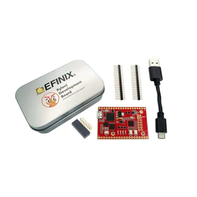
-
XYLONI
Efinix, Inc.
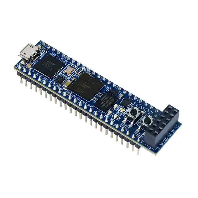
-
410-328-35
Digilent, Inc.
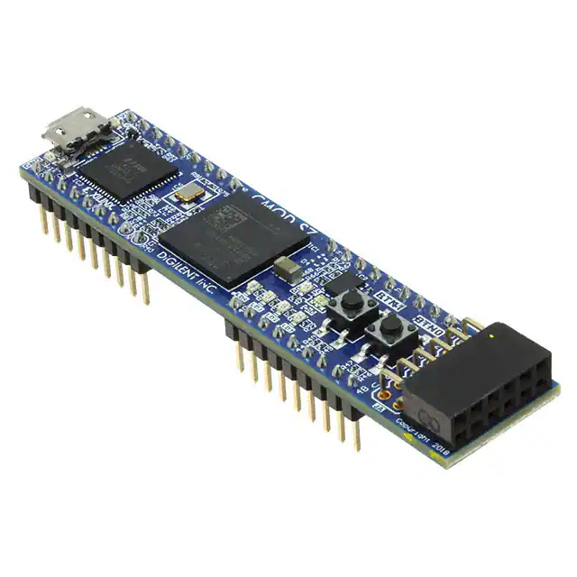
-
410-376
Digilent, Inc.
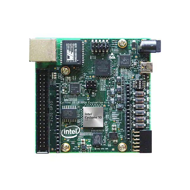
-
EK-10CL025U256
Intel
-
P0082
Terasic Inc.
-
SLG4DVKADV
Renesas
-
TEBA0841-02
Trenz Electronic GmbH
-
MPFS-DISCO-KIT
Microchip Technology
-
P0466
Terasic Inc.
-
410-370
Digilent, Inc.
Tech Hub

A practical engineering and sourcing framework covering lifecycle verification, lifetime-buy calculations, replacement qualification, supplier checks and counterfeit-risk controls.

TTL and CMOS logic families differ in thresholds, loading, output drive, power and timing. This engineering guide compares 74HC and 74HCT, calculates noise margins and checks 3.3 V/5 V compatibility.

A practical engineering guide to 3.3V and 5V logic compatibility, input thresholds, resistor dividers, translator ICs, MOSFET level shifting, I2C pull-ups, timing limits and power-sequencing risks.

The 74HC595 uses push-pull logic outputs, while the TPIC6B595 uses 50 V open-drain DMOS sinks for higher-power loads. This guide compares timing, current limits, 3.3 V interfacing, load wiring, thermal…

The 74HC595 converts serial data into eight stable parallel outputs. This guide covers pin functions, shift and storage timing, OE and MR behavior, drive-current limits, cascading, voltage compatibilit…

A technical comparison of level-sensitive latches and edge-triggered flip-flops, covering timing windows, setup and hold limits, master–slave operation, time borrowing, race-through, HDL inference and…

A D latch stores one bit while Enable controls when data can pass. This reference covers gate-level operation, truth tables, transparency, setup and hold timing, LE versus OE, common ICs and practical …

An SR latch stores one bit through cross-coupled feedback. This engineering reference covers NOR and NAND implementations, truth tables, forbidden-state recovery, gated operation, switch debouncing, fa…

Latch circuits retain one bit through feedback. This technical reference covers SR and D latches, truth tables, transparency, timing limits, latch-versus-flip-flop behavior, applications and common log…

An engineering guide to LED driver operation, constant-current and constant-voltage outputs, linear and switching topologies, dimming, IC selection, calculations, replacement compatibility, and fault c…


