
 My Inquiry
 My Account


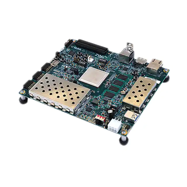
AMD EK-U1-ZCU104-G
- Part No.:
- EK-U1-ZCU104-G
- Manufacturer:
- AMD
- Package:
- Datasheet:
-
 EK-U1-ZCU104-G.pdf
- Description:
- XILINX ZYNQ ULTRASCALE+ ZCU104 P
- Quantity:
- Payment:

- Shipping:

Inventory:3,323
Please send an inquiry. Send us your inquiry, and we will respond immediately.
Product details
Overview
Ek-U1-ZCU104-G is the official Xilinx Zynq UltraScale+ MPSoC Evaluation Kit, designed for rapid prototyping and development of heterogeneous embedded vision, AI inference, and reconfigurable system-on-chip applications. It integrates the XCZU7EV-FFVC1156 FPGA/ARM SoC, 4GB DDR4 SODIMM memory, dual Gigabit Ethernet, USB 3.0, HDMI I/O, and pre-validated SDSoC™ toolchain support with OpenCV and live sensor interfaces.
For engineers reviewing the EK-U1-ZCU104-G datasheet, pinout, applications, or equivalent options, this page delivers verified board-level specifications, self-test procedures, power configuration requirements, SDSoC license redemption steps, and hardware validation workflows for reVISION-based embedded vision deployment.
Technical Context
The EK-U1-ZCU104-G implements a full Zynq UltraScale+ MPSoC platform with quad-core ARM Cortex-A53 (application processor), dual-core Cortex-R5F (real-time processor), Mali-400 GPU, and programmable logic fabric based on UltraScale+ architecture. It supports boot from QSPI flash (32-bit mode), JTAG debugging via USB-JTAG interface, and PCIe Gen2 x4 root port operation.
Hardware validation includes built-in self-test (BIST) covering clock integrity, PL-DDR4 memory, EEPROM, I²C peripherals, DIP switch inputs (SW13), pushbutton inputs (SW14–SW18), and PL GPIO LED outputs. Power sequencing is managed by integrated PMICs with monitored Power Good signals and VADJ control disabled by default.
Key Specifications
| Parameter | Value and Actual Design Meaning |
|---|---|
| MPSoC Device | XCZU7EV-FFVC1156: 7EV speed grade, 1156-pin flip-chip BGA, integrating ARM A53/R5F cores + UltraScale+ PL |
| Memory | 4GB DDR4 SODIMM (2400 MT/s), 256MB QSPI flash (32-bit addressable), 64KB on-chip SRAM per R5F core |
| Video Interfaces | HDMI 2.0 transmitter (TX) and receiver (RX), supporting up to 4K@30fps; MIPI CSI-2 connector for camera sensors |
| Connectivity | Dual 1Gbps Ethernet PHYs (RGMII), USB 3.0 host/device, PCIe Gen2 x4 root port, UART-to-USB bridge |
| Power Input | 12V DC via 6-pin terminal block (J52); regulated rails include 12V, 5V, 3.3V, 1.8V, 1.2V, and 0.85V for PL/VCCINT |
| Debug & Programming | Xilinx USB-JTAG interface (Xilinx Virtual Cable), JTAG header (2x10), SWD for R5F cores, and serial console over USB-UART |
Availability
EK-U1-ZCU104-G is available at Aetrix Electronics and suitable for embedded vision evaluation, AI accelerator prototyping, and reconfigurable H.264/H.265 video processing applications requiring stable component supply, long-term design support, and validated toolchain integration.
Supply support for EK-U1-ZCU104-G includes scheduled delivery planning, volume procurement assistance, BOM continuity management, traceable sourcing, and lifecycle availability coordination for OEM customers, industrial embedded developers, connected-device designers, and electronics production programs.
Manufacturer
Xilinx (now part of AMD) is a semiconductor company specializing in adaptive computing platforms, including FPGAs, MPSoCs, and ACAPs for high-performance, low-latency, and power-efficient system design.
The ZCU104 Evaluation Kit belongs to Xilinx's reVISION™ platform family, engineered specifically to accelerate embedded vision and machine learning inference using tightly coupled ARM processors and programmable logic-enabling real-time sensor fusion, OpenCV acceleration, and hardware-software co-design.
FAQ
What is the primary purpose of the EK-U1-ZCU104-G evaluation kit?
The EK-U1-ZCU104-G evaluation kit enables rapid development and validation of Zynq UltraScale+ MPSoC-based systems, especially for embedded vision and AI applications. It provides pre-integrated hardware-including the XCZU7EV device, DDR4 memory, HDMI, Ethernet, and USB 3.0-and out-of-box SDSoC™ toolflow with OpenCV libraries and live sensor support. Engineers use the EK-U1-ZCU104-G to prototype, benchmark, and deploy reVISION-based designs without custom board development.
Does the EK-U1-ZCU104-G support H.264/H.265 video encoding and decoding?
Yes, the EK-U1-ZCU104-G supports H.264/H.265 video processing via the integrated Video Codec Unit (VCU) inside the XCZU7EV device. The VCU is accessible through LogiCORE IP (PG252) and validated reference designs included with the kit. Real-time 4K@30fps decode and encode are achievable when combined with the HDMI TX/RX interfaces and DDR4 bandwidth-making the EK-U1-ZCU104-G suitable for video analytics and streaming applications.
How do I run the built-in self-test (BIST) on the EK-U1-ZCU104-G?
To run the BIST on the EK-U1-ZCU104-G, set SW6 to QSPI32 mode (DIP switches 1–4 = ON/OFF/ON/ON), apply 12V power via J52, and verify green Power Good LEDs and DONE LED illumination. The BIST starts automatically after configuration. Tests include Clock, BRAM, PL-DDR4, EEPROM, I²C, DIP switch (SW13), and pushbutton (SW14–SW18) validation-with status indicated by PL GPIO LEDs. No host PC is required for basic BIST execution.
Is an SDSoC license included with the EK-U1-ZCU104-G, and how is it redeemed?
Yes, the EK-U1-ZCU104-G includes a node-locked, device-locked SDSoC development environment license voucher for the XCZU7EV device. To redeem it, visit www.xilinx.com/getlicense, enter the printed voucher code from the Quick Start Guide, and associate it with your Xilinx account. The license is valid for one year from purchase and generates an email-delivered license file. This enables full SDSoC compilation, profiling, and hardware/software co-simulation for the EK-U1-ZCU104-G platform.
What debug and programming interfaces does the EK-U1-ZCU104-G provide?
The EK-U1-ZCU104-G provides multiple debug and programming interfaces: Xilinx USB-JTAG (Virtual Cable) for PL and PS configuration, a standard 2×10-pin JTAG header for external debuggers, SWD for Cortex-R5F cores, and a UART-to-USB bridge for serial console access. These interfaces allow full visibility into both programmable logic and ARM subsystems during development-essential for firmware bring-up, kernel debugging, and hardware verification on the EK-U1-ZCU104-G.
EK-U1-ZCU104-G Specifications
- Product attributes
- Attribute value
- Manufacturer:
- AMD
- Series:
- Zynq® UltraScale+™
- Packaging:
- Box
- Product Status:
- Active
- Type:
- FPGA + MCU/MPU SoC
- For Use With/Related Products:
- XCZU7EV
- Platform:
- Zynq UltraScale+ MPSoC ZCU104
- Contents:
- Board(s), Cable(s), Power Supply, Accessories
EK-U1-ZCU104-G FAQ
1.How can I place an order for EK-U1-ZCU104-G through Aetrix?
Please submit a Request for Quotation (RFQ) for EK-U1-ZCU104-G on Aetrix. Our sales agent will provide a competitive quotation and guide you through the order confirmation once you accept the terms.
2.Are the price and stock information for EK-U1-ZCU104-G reliable?
The price and inventory of EK-U1-ZCU104-G are updated periodically and may fluctuate due to market conditions. Stock and pricing data are typically refreshed every 24 hours. Quotation validity for EK-U1-ZCU104-G is usually 5 days.
3.What payment methods are accepted for EK-U1-ZCU104-G?
We accept Wire Transfer, PayPal, Credit Card, Western Union, MoneyGram, and Escrow for EK-U1-ZCU104-G transactions.
Note: Certain payment methods may incur a processing fee.
4.How is shipping managed for EK-U1-ZCU104-G?
EK-U1-ZCU104-G orders can be shipped via leading logistics carriers, including DHL, UPS, FedEx, TNT, or Registered Mail.
Once your EK-U1-ZCU104-G order is processed, you will receive an email with the shipment details and tracking number.
Note: Tracking information may take up to 24 hours to appear. Express delivery typically takes 3–5 business days.
5.How can I obtain technical support or documentation for EK-U1-ZCU104-G?
For technical support, including EK-U1-ZCU104-G datasheets, pinout diagrams, or application guidance, please contact our engineering support team. They can provide detailed documentation and assistance for your EK-U1-ZCU104-G requirements.
6.How does Aetrix verify that EK-U1-ZCU104-G is sourced from the original manufacturer or authorized distributors?
All EK-U1-ZCU104-G products on Aetrix are procured from qualified distributors and authorized channels. Our dedicated quality assurance team conducts strict verification, including traceability checks and, if necessary, third-party testing. This ensures that EK-U1-ZCU104-G meets industry standards.
7.What is the process for return or replacement of EK-U1-ZCU104-G?
All EK-U1-ZCU104-G units undergo pre-shipment inspection (PSI). If there is an issue with EK-U1-ZCU104-G, returns or replacements are accepted under the following conditions:
1.Quantity discrepancies, incorrect items, or visible external defects (such as breakage or corrosion), acknowledged by Aetrix.
2.The issue is reported within 90 days of delivery.
3.The EK-U1-ZCU104-G part is unused and in its original packaging.
Return procedure for EK-U1-ZCU104-G:
1.Submit a request within 90 days.
2.Obtain a Return Material Authorization (RMA) from Aetrix.
EK-U1-ZCU104-G Tags

-
EK-10M08E144
Intel
-
DK-DEV-10M08E144-B
Intel
-
XYLONI
Efinix, Inc.
-
410-328-35
Digilent, Inc.
-
410-376
Digilent, Inc.
-
EK-10CL025U256
Intel
-
P0082
Terasic Inc.
-
SLG4DVKADV
Renesas
-
TEBA0841-02
Trenz Electronic GmbH
-
MPFS-DISCO-KIT
Microchip Technology
-
P0466
Terasic Inc.
-
410-370
Digilent, Inc.
Tech Hub

A practical engineering and sourcing framework covering lifecycle verification, lifetime-buy calculations, replacement qualification, supplier checks and counterfeit-risk controls.

TTL and CMOS logic families differ in thresholds, loading, output drive, power and timing. This engineering guide compares 74HC and 74HCT, calculates noise margins and checks 3.3 V/5 V compatibility.

A practical engineering guide to 3.3V and 5V logic compatibility, input thresholds, resistor dividers, translator ICs, MOSFET level shifting, I2C pull-ups, timing limits and power-sequencing risks.

The 74HC595 uses push-pull logic outputs, while the TPIC6B595 uses 50 V open-drain DMOS sinks for higher-power loads. This guide compares timing, current limits, 3.3 V interfacing, load wiring, thermal…

The 74HC595 converts serial data into eight stable parallel outputs. This guide covers pin functions, shift and storage timing, OE and MR behavior, drive-current limits, cascading, voltage compatibilit…

A technical comparison of level-sensitive latches and edge-triggered flip-flops, covering timing windows, setup and hold limits, master–slave operation, time borrowing, race-through, HDL inference and…

A D latch stores one bit while Enable controls when data can pass. This reference covers gate-level operation, truth tables, transparency, setup and hold timing, LE versus OE, common ICs and practical …

An SR latch stores one bit through cross-coupled feedback. This engineering reference covers NOR and NAND implementations, truth tables, forbidden-state recovery, gated operation, switch debouncing, fa…

Latch circuits retain one bit through feedback. This technical reference covers SR and D latches, truth tables, transparency, timing limits, latch-versus-flip-flop behavior, applications and common log…

An engineering guide to LED driver operation, constant-current and constant-voltage outputs, linear and switching topologies, dimming, IC selection, calculations, replacement compatibility, and fault c…


