
 My Inquiry
 My Account


STMicroelectronics E-L6563TR

- Part No.:
- E-L6563TR
- Manufacturer:
- STMicroelectronics
- Category:
- PFC (Power Factor Correction)
- Package:
- 14-SOIC (0.154", 3.90mm Width)
- Datasheet:
-
 E-L6563TR.pdf
- Description:
- IC PFC CTRLR TRANSITION 14SO
- Quantity:
- Payment:

- Shipping:

Inventory:3,166
Please send an inquiry. Send us your inquiry, and we will respond immediately.
Product details
Overview
E-L6563TR from STMicroelectronics is an advanced transition-mode (TM) power factor correction (PFC) controller in SO-14 package, featuring 1.5% internal voltage reference (@TJ = 25°C), ≤90 µA start-up current, and -600/+800 mA totem-pole gate driver. It implements input voltage feedforward (1/V²), tracking boost, and latched feedback loop failure protection. Designed for >350W IEC61000-3-2-compliant AC-DC pre-regulators in desktop PCs and high-end adapters.
For engineers reviewing the E-L6563TR datasheet, E-L6563TR pinout, E-L6563TR application, or E-L6563TR equivalent, key selection criteria include its inductor saturation detection (L6563-specific), dual OVP architecture (static + dynamic), PFC_OK latched disable interface, and compatibility with cascaded PWM controllers for system-level fault coordination.
Technical Context
The E-L6563TR employs a current-mode TM control architecture with a highly linear multiplier and dedicated 1/V² feedforward path to minimize THD across wide input voltage and load ranges. Its error amplifier uses a precision 2.5 V reference with ±0.035 V tolerance at 25°C and 60–80 dB open-loop gain.
It integrates dual protection logic: PFC_OK pin triggers latched shutdown above 2.5 V (feedback failure), while CS pin detects inductor saturation at 1.7 V (L6563-only function). The RUN pin enables brownout detection via VFF-derived thresholding, and PWM_LATCH/PWM_STOP provide coordinated fault signaling to downstream DC-DC controllers.
Key Specifications
| Parameter | Value and Actual Design Meaning |
|---|---|
| Voltage Reference | 2.5 V ±1.5% @ TJ = 25°C - ensures stable output voltage regulation with minimal drift over temperature |
| Start-up Current | ≤90 µA @ VCC = 10 V - enables reliable startup from high-impedance auxiliary supplies |
| Quiescent Current | ≤5 mA during operation - minimizes no-load losses in energy-efficient SMPS designs |
| Gate Driver Output | +600 mA / -800 mA sink-source - directly drives high-Ciss MOSFETs without external buffers |
| OVP Threshold | 2.5 V (latched) on PFC_OK pin - provides fail-safe shutdown if feedback loop opens or sets incorrect voltage |
| CS Saturation Detection | 1.7 V threshold on pin 4 - halts switching and asserts PWM_LATCH upon boost inductor core saturation |
| UVLO Thresholds | VON = 12 V, VOFF = 9.5 V - ensures clean power sequencing with 2.7 V hysteresis |
Pinout & Package
SO-14 surface-mount package with standard JEDEC outline, 1.27 mm pitch, and thermal resistance RthJA = 120 °C/W. Pin 12 serves as common ground return for both analog circuitry and gate driver.
| Pin/Terminal | Circuit Role | Design Meaning |
|---|---|---|
| 1 (INV) | Inverting input of voltage error amplifier | Accepts resistor-divider feedback; sinks programmable current from TBO for tracking boost |
| 4 (CS) | Current sense comparator input | Detects MOSFET conduction current; triggers latched shutdown at 1.7 V for inductor saturation |
| 7 (PFC_OK) | Output voltage monitor / disable input | Latched shutdown above 2.5 V (feedback failure); active-low disable below 0.2 V |
| 8 (PWM_LATCH) | Fault signaling output | Open-drain high when PFC_OK > 2.5 V or CS > 1.7 V - used to latch-disable downstream PWM controller |
| 13 (GD) | Gate driver output | Totem-pole stage with active pull-down during UVLO; clamped to ~12 V for MOSFET gate protection |
| 14 (VCC) | Supply input | Self-limited to 25 V Zener clamp; powers both signal and driver sections |
Key Features
| Feature | Design Value |
|---|---|
| Inductor saturation detection | Hardware-based 1.7 V threshold on CS pin (L6563 only) prevents destructive overcurrent during boost choke saturation |
| Tracking Boost function | Adjustable output voltage scaling via TBO pin current - maintains optimal VOUT/VIN ratio across universal AC input range |
| Two-stage OVP | Dynamic OVP (17–23 µA trigger) + static OVP (2.15 V threshold) - protects against transient surges and steady-state regulator faults |
| Feedback failure protection | Latched shutdown via PFC_OK > 2.5 V with automatic consumption reduction to ~250 µA - eliminates risk of uncontrolled overvoltage |
| Voltage feedforward (1/V²) | Internal RMS line sensing via VFF pin - compensates loop gain variation across 90–264 VAC, enabling <5% THD at full load |
Applications
| Desktop PC Power Supply | Server PSU Pre-regulator |
|---|---|
Use Scenario: 500–800W ATX/SSI-compliant power supply with active PFC stage preceding LLC resonant DC-DC converter. IC Role / Device Role / Timing Role: Transition-mode PFC controller regulating 380–400 VDC bus; synchronizes MOSFET turn-on with zero-current detection on boost inductor. Use Value: Enables EN61000-3-2 Class D compliance at full load with THD <4.5%, reducing EMI filter size and cost. |
Use Scenario: Redundant 1 kW server PSU requiring high reliability, low standby loss, and coordinated fault response between PFC and downstream converters. IC Role / Device Role / Timing Role: Primary PFC controller interfacing with PWM_LATCH to halt secondary-stage operation during PFC faults (e.g., feedback open). Use Value: Latched PFC_OK shutdown and PWM_LATCH assertion prevent catastrophic overvoltage on 12 V/54 V rails during regulator failure. |
| High-End AC Adapter | IEC61000-3-2 Compliant SMPS |
Use Scenario: 350–450W medical-grade or broadcast equipment adapter requiring ultra-low THD and robust brownout recovery. IC Role / Device Role / Timing Role: PFC controller using RUN pin tied to VFF for automatic brownout disable below 85 VAC RMS; resumes after 150 ms delay. Use Value: ≤90 µA start-up current and 0.52 V RUN threshold enable seamless restart after brief AC dips without capacitor recharge delay. |
Use Scenario: Industrial motor drive front-end or test equipment SMPS requiring >350W PFC with JEITA-MITI harmonic limits. IC Role / Device Role / Timing Role: Core PFC controller implementing 1/V² feedforward and THD optimizer circuit to meet <8% THD at 20% load. Use Value: Multiplier gain stability (±5% over -25°C to +125°C) ensures consistent current shaping across ambient temperature extremes. |
Equivalent & Alternatives
The following parts are listed as comparable options for similar transition-mode PFC controller applications.
| Alternative Part | Technical Difference | Application Difference | Selection Advice |
|---|---|---|---|
| ICE3PCS01G | No inductor saturation detection; fixed 2.5 V OVP (non-latched); lower gate drive (±500 mA) | Lacks hardware-level saturation protection and latched feedback failure response | Select when cost sensitivity outweighs need for saturation fault coverage in non-critical systems |
| L6564TR | Fixed-off-time TM control (no ZCD input); no PFC_OK latch; higher quiescent current (7 mA) | Requires external zero-cross detection; no direct interface to downstream PWM latch signals | Prefer for simpler designs where coordinated multi-stage fault handling is not required |
Compared with ICE3PCS01G and L6564TR, the E-L6563TR uniquely combines latched feedback failure protection, inductor saturation detection, and dedicated PWM_LATCH signaling-making it the only choice for safety-critical >350W PFC stages requiring guaranteed fault containment.
Availability
E-L6563TR is available at Aetrix Electronics and suitable for desktop PC power supplies, server PSUs, and IEC61000-3-2-compliant industrial SMPS requiring stable component supply, long-term lifecycle support, and traceable sourcing.
Supply support for E-L6563TR includes scheduled delivery planning, volume procurement assistance, BOM continuity management, traceable sourcing, and lifecycle availability coordination for OEM customers, industrial embedded developers, connected-device designers, and electronics production programs.
Manufacturer
STMicroelectronics is a global semiconductor leader headquartered in Geneva, specializing in power management, analog, and microcontroller solutions for industrial, automotive, and consumer markets.
The L6563 product line delivers high-precision, low-power-transition-mode PFC controllers targeting >350W AC-DC conversion systems requiring EN61000-3-2 compliance, robust fault handling, and seamless integration with downstream DC-DC stages.
FAQ
What is the functional difference between E-L6563TR and E-L6563ATR?
The E-L6563TR includes inductor saturation detection (via 1.7 V threshold on CS pin) and a latched PWM_LATCH signal triggered by either PFC_OK overvoltage or CS saturation events. The E-L6563ATR omits the saturation detection circuit entirely and lacks the associated PWM_LATCH assertion on CS faults-making the TR variant mandatory for designs requiring hardware-level boost choke protection.
How does the Tracking Boost function operate on E-L6563TR?
The Tracking Boost function uses a buffered VFF voltage on pin 6 (TBO) to sink programmable current from pin 1 (INV), dynamically adjusting the PFC output voltage setpoint in proportion to the RMS input voltage. A resistor from TBO to GND sets the current; typical values yield 380 V at 230 VAC and 350 V at 115 VAC, optimizing efficiency across universal input range.
Can E-L6563TR be used without the PFC_OK pin connection?
Yes-pin 7 (PFC_OK) may be tied to a DC voltage between 0.26 V and 2.5 V to disable both latch-off and disable functions. However, doing so forfeits critical feedback loop failure protection. For safety-certified designs, ST recommends connecting PFC_OK to the output divider to retain latched shutdown on open-loop conditions.
What is the purpose of the RUN pin in E-L6563TR?
The RUN pin (10) provides remote ON/OFF control with brownout detection capability. When tied to VFF via a resistor divider, it disables the IC below 0.52 V (≈85 VAC RMS), then re-enables at 0.6 V after a 150 µs start timer. This enables automatic AC undervoltage shutdown without external circuitry, supporting Energy Star and Blue Angel compliance.
E-L6563TR Specifications
- Product attributes
- Attribute value
- Manufacturer:
- STMicroelectronics
- Series:
- -
- Package/Case:
- 14-SOIC (0.154", 3.90mm Width)
- Packaging:
- Tape & Reel (TR)
- Product Status:
- Obsolete
- Mode:
- Discontinuous (Transition)
- Frequency - Switching:
- -
- Current - Startup:
- 50 µA
- Voltage - Supply:
- 10.3V ~ 22V
- Operating Temperature:
- -25°C ~ 125°C
- Grade:
- -
- Qualification:
- -
- Mounting Type:
- Surface Mount
- Supplier Device Package:
- 14-SO
E-L6563TR FAQ
1.How can I place an order for E-L6563TR through Aetrix?
Please submit a Request for Quotation (RFQ) for E-L6563TR on Aetrix. Our sales agent will provide a competitive quotation and guide you through the order confirmation once you accept the terms.
2.Are the price and stock information for E-L6563TR reliable?
The price and inventory of E-L6563TR are updated periodically and may fluctuate due to market conditions. Stock and pricing data are typically refreshed every 24 hours. Quotation validity for E-L6563TR is usually 5 days.
3.What payment methods are accepted for E-L6563TR?
We accept Wire Transfer, PayPal, Credit Card, Western Union, MoneyGram, and Escrow for E-L6563TR transactions.
Note: Certain payment methods may incur a processing fee.
4.How is shipping managed for E-L6563TR?
E-L6563TR orders can be shipped via leading logistics carriers, including DHL, UPS, FedEx, TNT, or Registered Mail.
Once your E-L6563TR order is processed, you will receive an email with the shipment details and tracking number.
Note: Tracking information may take up to 24 hours to appear. Express delivery typically takes 3–5 business days.
5.How can I obtain technical support or documentation for E-L6563TR?
For technical support, including E-L6563TR datasheets, pinout diagrams, or application guidance, please contact our engineering support team. They can provide detailed documentation and assistance for your E-L6563TR requirements.
6.How does Aetrix verify that E-L6563TR is sourced from the original manufacturer or authorized distributors?
All E-L6563TR products on Aetrix are procured from qualified distributors and authorized channels. Our dedicated quality assurance team conducts strict verification, including traceability checks and, if necessary, third-party testing. This ensures that E-L6563TR meets industry standards.
7.What is the process for return or replacement of E-L6563TR?
All E-L6563TR units undergo pre-shipment inspection (PSI). If there is an issue with E-L6563TR, returns or replacements are accepted under the following conditions:
1.Quantity discrepancies, incorrect items, or visible external defects (such as breakage or corrosion), acknowledged by Aetrix.
2.The issue is reported within 90 days of delivery.
3.The E-L6563TR part is unused and in its original packaging.
Return procedure for E-L6563TR:
1.Submit a request within 90 days.
2.Obtain a Return Material Authorization (RMA) from Aetrix.
E-L6563TR Tags

-
ICE2PCS01GXUMA1
Infineon Technologies

-
NCP1654BD133R2G
onsemi
-
MC33262DR2G
onsemi
-
ICE3PCS03GXUMA1
Infineon Technologies
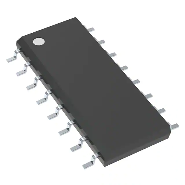
-
NCP1631DR2G
onsemi

-
L4981BD013TR
STMicroelectronics
-
UCC28070DWR
Texas Instruments

-
UCC28070PWR
Texas Instruments

-
UC3854DWTR
Texas Instruments
-
L4981AD013TR
STMicroelectronics

-
UCC2817D
Texas Instruments
-
UC2854BDWTR
Texas Instruments
Tech Hub

A practical engineering and sourcing framework covering lifecycle verification, lifetime-buy calculations, replacement qualification, supplier checks and counterfeit-risk controls.

TTL and CMOS logic families differ in thresholds, loading, output drive, power and timing. This engineering guide compares 74HC and 74HCT, calculates noise margins and checks 3.3 V/5 V compatibility.

A practical engineering guide to 3.3V and 5V logic compatibility, input thresholds, resistor dividers, translator ICs, MOSFET level shifting, I2C pull-ups, timing limits and power-sequencing risks.

The 74HC595 uses push-pull logic outputs, while the TPIC6B595 uses 50 V open-drain DMOS sinks for higher-power loads. This guide compares timing, current limits, 3.3 V interfacing, load wiring, thermal…

The 74HC595 converts serial data into eight stable parallel outputs. This guide covers pin functions, shift and storage timing, OE and MR behavior, drive-current limits, cascading, voltage compatibilit…

A technical comparison of level-sensitive latches and edge-triggered flip-flops, covering timing windows, setup and hold limits, master–slave operation, time borrowing, race-through, HDL inference and…

A D latch stores one bit while Enable controls when data can pass. This reference covers gate-level operation, truth tables, transparency, setup and hold timing, LE versus OE, common ICs and practical …

An SR latch stores one bit through cross-coupled feedback. This engineering reference covers NOR and NAND implementations, truth tables, forbidden-state recovery, gated operation, switch debouncing, fa…

Latch circuits retain one bit through feedback. This technical reference covers SR and D latches, truth tables, transparency, timing limits, latch-versus-flip-flop behavior, applications and common log…

An engineering guide to LED driver operation, constant-current and constant-voltage outputs, linear and switching topologies, dimming, IC selection, calculations, replacement compatibility, and fault c…


