
 My Inquiry
 My Account


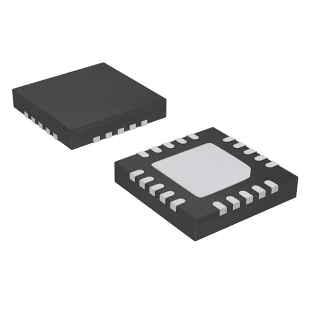
Renesas EL7586AILZ-T13
- Part No.:
- EL7586AILZ-T13
- Manufacturer:
- Renesas
- Category:
- Special Purpose Regulators
- Package:
- 20-VFQFN Exposed Pad
- Datasheet:
-
 EL7586AILZ-T13.pdf
- Description:
- IC REG CONV TFT LCD 4OUT 20QFN
- Quantity:
- Payment:

- Shipping:

Inventory:4,977
Please send an inquiry. Send us your inquiry, and we will respond immediately.
Product details
Overview
EL7586AILZ-T13 from Intersil is a highly integrated TFT-LCD power supply IC featuring a 2A boost converter, two positive LDO controllers (VON and VLOGIC), and one negative LDO controller (VOFF), all operating across –40°C to +85°C. It delivers 1% regulation on all outputs, supports up to 20V boost output, and enables programmable startup sequencing for LCD panel bias rails in large-format displays.
For engineers reviewing the EL7586AILZ-T13 datasheet, EL7586AILZ-T13 pinout, EL7586AILZ-T13 application, or EL7586AILZ-T13 equivalent, this page provides verified technical context, validated pin functions, confirmed sequencing behavior (immediate VLOGIC enable), fault protection timing, and real-world design constraints for TFT-LCD power systems.
Technical Context
The EL7586AILZ-T13 implements a fixed-frequency 1 MHz current-mode PWM boost regulator with internal 2A N-channel FET, supporting both P-mode and PI-mode operation via CINT pin configuration. Its three independent LDO controllers drive external pass transistors for VON (+15V typical), VOFF (–5V typical), and VLOGIC (+2.5V typical) with dedicated feedback pins (FBP, FBN, FBL) referenced to 1.2V, 0.2V, and 1.2V respectively.
Startup sequencing is hardware-defined: EL7586AILZ-T13 powers VLOGIC immediately at EN assertion (independent of EN state), then sequences VOFF and VON using CDLY capacitor timing. Fault detection latches off all outputs until input or EN cycling, with fault timeout set by CDLY and monitored on DELB and PG pins.
Key Specifications
| Parameter | Value and Actual Design Meaning |
|---|---|
| Boost Output Range | 5.5V to 20V - sets AVDD rail for LCD source drivers; requires external resistor divider on FBB pin. |
| VLOGIC Regulation Voltage | 1.176V to 1.224V at 1mA - references external PNP pass transistor to generate stable logic supply (e.g., 2.5V). |
| VOFF Feedback Reference | 0.173V to 0.233V at 0.2mA - low-voltage reference enabling precise –5V generation via external NPN pass device. |
| Startup Delay (CDLY = 0.22µF) | 30ms turn-on delay - defines minimum time before first output activation; critical for charge-pump settling. |
| Fault Timeout Duration | 50ms - time window after which latch-off occurs if DELB or PG fails to reach threshold during startup. |
| Oscillator Frequency | 900kHz to 1100kHz - determines inductor size and ripple; enables use of compact 6.8µH ceramic-choked designs. |
| Operating Temperature | –40°C to +85°C - qualified for industrial and commercial LCD monitor/TV environments without derating. |
Pinout & Package
EL7586AILZ-T13 is housed in a 20-lead 4mm × 4mm QFN package with exposed thermal pad (PKG DWG # MDP0046), RoHS-compliant Pb-free plus anneal finish, and moisture sensitivity level (MSL) compatible with standard Pb-free reflow profiles.
| Pin/Terminal | Circuit Role | Design Meaning |
|---|---|---|
| 1 CDLY | Sequencing & fault timing capacitor node | Connects to GND to set startup delay (tON = 30ms @ 0.22µF) and fault timeout (tFAULT = 50ms). |
| 2 DELB | Open-drain gate drive for VBOOST delay FET | Sinks 50µA initially, then ~1.2mA to pull low; used to delay AVDD ramp after VOFF stabilization. |
| 3,4 LX1/LX2 | Internal boost FET drain terminals | LX1 is active switch node; LX2 is no-connect on EL7586AILZ-T13 (not used in A-version). |
| 5 DRVP | Open-drain N-FET base drive for VON LDO | Drives external PNP pass transistor (e.g., FMMT549); max sink current 4mA. |
| 6 FBP | VON output voltage feedback input | Regulates to 1.2V nominal; fault trips at 0.82–0.92V falling - detects VON undervoltage. |
| 7 DRVL | Open-drain N-FET base drive for VLOGIC LDO | Drives external PNP pass device; supports up to 500mA load with 16mA max sink capability. |
| 8 FBL | VLOGIC output voltage feedback input | Regulates to 1.2V nominal; fault threshold 0.82–0.92V falling - ensures logic rail integrity. |
| 9,17 SGND | Low-noise signal ground reference | Must be isolated from PGND; connects to VREF bypass cap and feedback resistors. |
| 10 DRVN | Open-drain P-FET base drive for VOFF LDO | Drives external NPN pass transistor; sources up to 4mA for –5V generation. |
| 11 FBN | VOFF output voltage feedback input | Regulates to 0.2V nominal; fault triggers at 0.38–0.48V falling - monitors negative rail stability. |
| 12,13 PGND | Power ground return for boost FET source | Must be low-inductance connection to LX and input/output capacitors; tied to thermal pad. |
| 14 VREF | Bandgap reference bypass | Requires 0.1µF ceramic cap to SGND; stabilizes internal 1.215V reference for all LDOs. |
| 15 CINT | Boost integrator output / mode select | Connect to VDD for P-mode; add 4.7nF to SGND for PI-mode - improves load regulation to 0.1%. |
| 16 FBB | Boost output voltage feedback input | Regulates to 1.205V nominal; fault trip at 0.9V - protects against overvoltage or open feedback. |
| 18 EN | Enable control input | Logic high (≥2.3V) enables device; floating or low disables - but VLOGIC remains active on EL7586A. |
| 19 VDD | Main supply input | Accepts 3V–5.5V; powers internal circuitry and sets UVLO threshold (typ. 2.8V). |
| 20 PG | Push-pull fault indicator / protection gate drive | High when enabled/fault-free; pulls low (~15µA → 1.2mA) to activate external protection FET Q1. |
Key Features
| Feature | Design Value |
|---|---|
| Integrated 2A boost FET | Eliminates external high-current MOSFET; reduces BOM count and layout area for AVDD generation. |
| Independent LDO controllers | Three separate feedback loops (FBP/FBL/FBN) allow simultaneous, non-interacting regulation of VON, VLOGIC, and VOFF rails. |
| Immediate VLOGIC enable | VLOGIC powers up instantly upon VDD application - no dependency on EN or sequencing - critical for early logic initialization. |
| Programmable sequencing | CDLY capacitor configures tON, tDEL1, tDEL2, and tFAULT; supports custom ramp order for panel reliability. |
| Full fault protection | Dedicated comparators monitor all four outputs; latch-off prevents damage during overvoltage, undervoltage, or thermal events. |
| Pb-free QFN package | 20-lead 4×4 mm RoHS-compliant package with exposed thermal pad - supports automated assembly and thermal management. |
Applications
| Large-Panel LCD Monitors (15"+) | LCD Television (up to 40"+) |
|---|---|
|
Use Scenario: Powering row/column driver ICs and timing controllers in 24"–32" desktop monitors requiring stable ±15V/2.5V rails. IC Role / Device Role / Timing Role: EL7586AILZ-T13 generates AVDD (12–15V), VON (+15V), VOFF (–5V), and VLOGIC (2.5V) with sequenced startup to prevent panel latch-up. Use Value: Integrated sequencing eliminates need for external timers or microcontrollers; 1% regulation ensures consistent gamma correction across brightness levels. |
Use Scenario: Bias supply for 32"–42" LCD TV panels where EMI, efficiency, and startup reliability are critical in consumer-grade designs. IC Role / Device Role / Timing Role: EL7586AILZ-T13 serves as primary multi-rail power manager, coordinating VBOOST→VOFF→VON ramp while maintaining VLOGIC from power-on. Use Value: PI-mode boost regulation (0.1% load regulation) minimizes AVDD droop during dynamic video scenes, preserving contrast ratio. |
| Notebook Display Panels (up to 16") | Industrial/Medical LCD Displays |
|
Use Scenario: Compact power solution for portable 12"–16" notebook displays where board space and thermal envelope are constrained. IC Role / Device Role / Timing Role: EL7586AILZ-T13 integrates boost + three LDO controllers into single QFN, reducing discrete count versus multi-IC solutions. Use Value: 4×4 mm footprint and internal 2A FET cut total solution size by >35% vs. discrete boost + dual LDO approach. |
Use Scenario: Reliable bias generation for diagnostic monitors and surgical display systems requiring long-term stability and fault resilience. IC Role / Device Role / Timing Role: EL7586AILZ-T13 provides latch-off fault protection and –40°C to +85°C operation for mission-critical display uptime. Use Value: Thermal shutdown (140°C) and fault timeout (50ms) prevent catastrophic failure during extended operation or ambient temperature excursions. |
Equivalent & Alternatives
The following parts are listed as comparable options for similar TFT-LCD power supply applications.
| Alternative Part | Technical Difference | Application Difference | Selection Advice |
|---|---|---|---|
| EL7586ILZ-T13 | Same pinout and package, but lacks immediate VLOGIC enable; VLOGIC follows full startup sequence only after EN assertion. | Not suitable where logic rail must power up before panel bias rails - e.g., timing controller initialization prior to gate driver enable. | Select EL7586ILZ-T13 only if VLOGIC sequencing dependency on EN is acceptable and cost is prioritized over flexibility. |
| RTQ2132B-QT | Single-chip quad-output PMIC (boost + 3 LDOs) with I²C programmability, higher integration, and 125°C junction rating. | Supports dynamic voltage scaling and telemetry; requires firmware integration unlike EL7586AILZ-T13's analog-only configuration. | Choose RTQ2132B-QT when digital control, diagnostics, or extended temperature range (>85°C ambient) are required. |
Compared with EL7586ILZ-T13, EL7586AILZ-T13 offers guaranteed VLOGIC availability at power-on - eliminating boot dependency on EN - while RTQ2132B-QT adds configurability at the cost of analog simplicity and legacy design compatibility.
Availability
EL7586AILZ-T13 is available at Aetrix Electronics and suitable for LCD monitors (15"+), LCD-TV (up to 40"+), and industrial LCD displays requiring stable component supply, long-lifecycle support, and RoHS-compliant packaging.
Supply support for EL7586AILZ-T13 includes scheduled delivery planning, volume procurement assistance, BOM continuity management, traceable sourcing, and lifecycle availability coordination for OEM customers, industrial embedded developers, connected-device designers, and electronics production programs.
Manufacturer
Intersil (now part of Renesas Electronics) is a semiconductor company specializing in precision analog, power management, and interface ICs for industrial, computing, and consumer electronics.
The EL7586A product line was designed specifically for TFT-LCD panel power management - integrating boost conversion and three independent LDO controllers to replace multi-chip discrete solutions in display subsystems.
FAQ
What is the key functional difference between EL7586AILZ-T13 and EL7586ILZ-T13?
The EL7586AILZ-T13 features immediate VLOGIC enable - its VLOGIC output activates as soon as VDD is applied, independent of the EN pin state. In contrast, EL7586ILZ-T13 requires EN assertion before any output, including VLOGIC, becomes active. This makes EL7586AILZ-T13 essential for designs where logic power must be available before panel bias sequencing begins. The EL7586AILZ-T13 retains full pin compatibility with EL7586ILZ-T13.
How does the EL7586AILZ-T13 implement fault protection and recovery?
The EL7586AILZ-T13 monitors all four regulated outputs (VBOOST, VON, VOFF, VLOGIC) via dedicated feedback comparators. Upon detecting an undervoltage or overvoltage condition - such as FBB < 0.9V or FBN < 0.38V - it latches off all outputs and drives PG high. Recovery requires cycling the input supply or toggling EN. Fault timeout is set by the CDLY capacitor (50ms default with 0.22µF), and DELB/PG pin behavior confirms fault status during startup.
Can EL7586AILZ-T13 support VBOOST outputs above 20V?
No - the EL7586AILZ-T13's internal boost FET is rated for ≤20V output. For VBOOST > 20V, a cascaded external MOSFET topology is required, as shown in Figure 27 of the datasheet. In that configuration, the internal FET drives the gate of an external high-voltage N-channel device, with LX connected to the source of the external FET. The EL7586AILZ-T13 itself does not regulate beyond 20V.
What is the role of the CINT pin on EL7586AILZ-T13, and how does it affect performance?
The CINT pin selects between P-mode (connect to VDD) and PI-mode (connect 4.7nF to SGND) for the boost regulator's error amplifier. PI-mode reduces load regulation error from 3% to 0.1% - critical for maintaining AVDD stability under varying panel current demands. P-mode simplifies layout but sacrifices regulation accuracy. Both modes retain the same 1MHz switching frequency and 2A current limit.
Is EL7586AILZ-T13 suitable for new designs, and what is its lifecycle status?
Yes - while the base EL7586 is marked "not recommended for new designs," the EL7586A variant (including EL7586AILZ-T13) remains actively supported by Renesas. It is listed in current distribution channels with full documentation, recommended replacement guidance, and no announced obsolescence. Designers should use EL7586AILZ-T13 - not EL7586ILZ-T13 - for all new TFT-LCD power applications.
EL7586AILZ-T13 Specifications
- Product attributes
- Attribute value
- Manufacturer:
- Renesas
- Series:
- -
- Package/Case:
- 20-VFQFN Exposed Pad
- Packaging:
- Tape & Reel (TR)
- Product Status:
- Obsolete
- Applications:
- Converter, TFT LCD
- Voltage - Input:
- 3V ~ 5V
- Number of Outputs:
- 4
- Voltage - Output:
- 5.5V ~ 20V
- Operating Temperature:
- -40°C ~ 85°C
- Grade:
- -
- Qualification:
- -
- Mounting Type:
- Surface Mount
- Supplier Device Package:
- 20-QFN (4x4)
EL7586AILZ-T13 FAQ
1.How can I place an order for EL7586AILZ-T13 through Aetrix?
Please submit a Request for Quotation (RFQ) for EL7586AILZ-T13 on Aetrix. Our sales agent will provide a competitive quotation and guide you through the order confirmation once you accept the terms.
2.Are the price and stock information for EL7586AILZ-T13 reliable?
The price and inventory of EL7586AILZ-T13 are updated periodically and may fluctuate due to market conditions. Stock and pricing data are typically refreshed every 24 hours. Quotation validity for EL7586AILZ-T13 is usually 5 days.
3.What payment methods are accepted for EL7586AILZ-T13?
We accept Wire Transfer, PayPal, Credit Card, Western Union, MoneyGram, and Escrow for EL7586AILZ-T13 transactions.
Note: Certain payment methods may incur a processing fee.
4.How is shipping managed for EL7586AILZ-T13?
EL7586AILZ-T13 orders can be shipped via leading logistics carriers, including DHL, UPS, FedEx, TNT, or Registered Mail.
Once your EL7586AILZ-T13 order is processed, you will receive an email with the shipment details and tracking number.
Note: Tracking information may take up to 24 hours to appear. Express delivery typically takes 3–5 business days.
5.How can I obtain technical support or documentation for EL7586AILZ-T13?
For technical support, including EL7586AILZ-T13 datasheets, pinout diagrams, or application guidance, please contact our engineering support team. They can provide detailed documentation and assistance for your EL7586AILZ-T13 requirements.
6.How does Aetrix verify that EL7586AILZ-T13 is sourced from the original manufacturer or authorized distributors?
All EL7586AILZ-T13 products on Aetrix are procured from qualified distributors and authorized channels. Our dedicated quality assurance team conducts strict verification, including traceability checks and, if necessary, third-party testing. This ensures that EL7586AILZ-T13 meets industry standards.
7.What is the process for return or replacement of EL7586AILZ-T13?
All EL7586AILZ-T13 units undergo pre-shipment inspection (PSI). If there is an issue with EL7586AILZ-T13, returns or replacements are accepted under the following conditions:
1.Quantity discrepancies, incorrect items, or visible external defects (such as breakage or corrosion), acknowledged by Aetrix.
2.The issue is reported within 90 days of delivery.
3.The EL7586AILZ-T13 part is unused and in its original packaging.
Return procedure for EL7586AILZ-T13:
1.Submit a request within 90 days.
2.Obtain a Return Material Authorization (RMA) from Aetrix.
EL7586AILZ-T13 Tags

-
TPS51206DSQR
Texas Instruments

-
TPS51200DRCR
Texas Instruments
-
TPS51200DRCT
Texas Instruments

-
TPS62740DSSR
Texas Instruments

-
TPS51100DGQR
Texas Instruments

-
NCP51200MNTXG
onsemi
-
NCP51400MNTXG
onsemi

-
RT9026GSP
Richtek USA Inc.

-
LP2998MRX/NOPB
Texas Instruments
-
TPS51200QDRCRQ1
Texas Instruments

-
DPA423GN-TL
Power Integrations
-
LM10011SD/NOPB
Texas Instruments
Tech Hub

TTL and CMOS logic families differ in thresholds, loading, output drive, power and timing. This engineering guide compares 74HC and 74HCT, calculates noise margins and checks 3.3 V/5 V compatibility.

A practical engineering guide to 3.3V and 5V logic compatibility, input thresholds, resistor dividers, translator ICs, MOSFET level shifting, I2C pull-ups, timing limits and power-sequencing risks.

The 74HC595 uses push-pull logic outputs, while the TPIC6B595 uses 50 V open-drain DMOS sinks for higher-power loads. This guide compares timing, current limits, 3.3 V interfacing, load wiring, thermal…

The 74HC595 converts serial data into eight stable parallel outputs. This guide covers pin functions, shift and storage timing, OE and MR behavior, drive-current limits, cascading, voltage compatibilit…

A technical comparison of level-sensitive latches and edge-triggered flip-flops, covering timing windows, setup and hold limits, master–slave operation, time borrowing, race-through, HDL inference and…

A D latch stores one bit while Enable controls when data can pass. This reference covers gate-level operation, truth tables, transparency, setup and hold timing, LE versus OE, common ICs and practical …

An SR latch stores one bit through cross-coupled feedback. This engineering reference covers NOR and NAND implementations, truth tables, forbidden-state recovery, gated operation, switch debouncing, fa…

Latch circuits retain one bit through feedback. This technical reference covers SR and D latches, truth tables, transparency, timing limits, latch-versus-flip-flop behavior, applications and common log…

An engineering guide to LED driver operation, constant-current and constant-voltage outputs, linear and switching topologies, dimming, IC selection, calculations, replacement compatibility, and fault c…

Operational amplifier guide covering op amp basics, feedback, ideal vs real op amps, common configurations, buffer circuits, offset, bias current, gain-bandwidth, slew rate, rail-to-rail limits and sel…


