
 My Inquiry
 My Account


Analog Devices Inc. EV1HMC349ALP4C
- Part No.:
- EV1HMC349ALP4C
- Manufacturer:
- Analog Devices Inc.
- Category:
- RF, RFID, Wireless Evaluation Boards
- Package:
- Datasheet:
-
 EV1HMC349ALP4C.pdf
- Description:
- BOARD EVALUATION HMC349ALP4C
- Quantity:
- Payment:

- Shipping:

Inventory:2,884
Please send an inquiry. Send us your inquiry, and we will respond immediately.
Product details
Overview
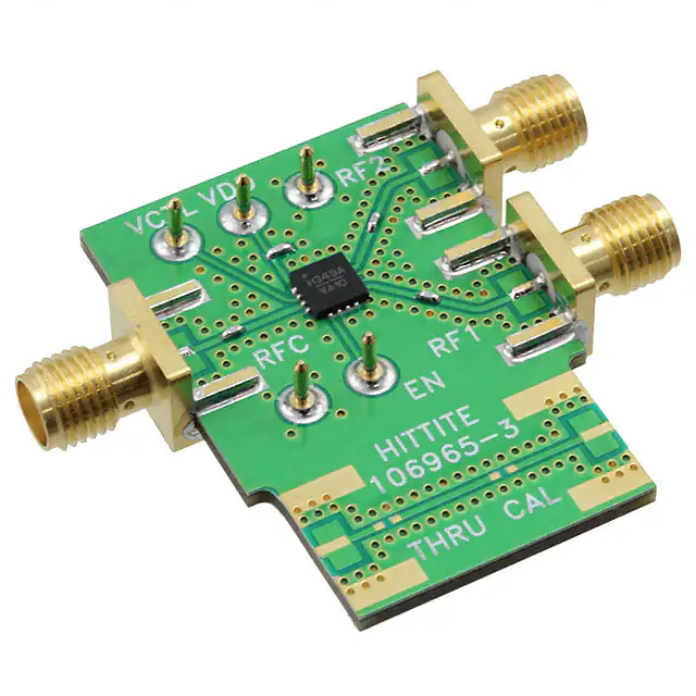
EV1HMC349ALP4C from Analog Devices is an evaluation board designed to characterize the HMC349ALP4CE GaAs SPDT RF switch, supporting 100 MHz to 4 GHz operation with 1.0 dB typical insertion loss and 62 dB isolation at 2 GHz. It enables rapid prototyping of high-isolation RF path switching in wireless infrastructure and test equipment.
For engineers reviewing the EV1HMC349ALP4C datasheet, EV1HMC349ALP4C pinout, EV1HMC349ALP4C application, or EV1HMC349ALP4C equivalent, this board provides full access to RFC, RF1, and RF2 SMA connectors, on-board 100 pF dc blocking capacitors, and a 4-layer Rogers RO4350/FR-4 hybrid PCB optimized for 50 Ω coplanar waveguide routing and thermal grounding.
Technical Context
The EV1HMC349ALP4C implements a 4-layer PCB with 0.5 oz copper, top-layer Rogers RO4350 (10 mil) for RF integrity, and FR-4 inner/bottom layers for structural stability. RF traces use 13-mil-width coplanar waveguide with 10-mil ground spacing to maintain 50 Ω impedance across the full 100 MHz–4 GHz band.
It integrates three PC-mount SMA connectors (J1: RFC, J2: RF2, J3: RF1), dedicated DC control pins (J4: CTRL, J8: EN, J5: VDD, J6/J7: GND), and plated-through vias densely arranged under the HMC349ALP4CE's exposed pad and RF paths to ensure low-inductance RF and thermal grounding.
Key Specifications
| Parameter | Value and Actual Design Meaning |
|---|---|
| RF Frequency Range | 100 MHz to 4 GHz - fully supports cellular, Wi-Fi, and test instrumentation bands without external matching. |
| RF Interface | SMA connectors on RFC, RF1, RF2 - enables direct connection to signal generators, spectrum analyzers, and antenna systems. |
| PCB Stack-up | 4-layer: RO4350 top (10 mil), FR-4 core & bottom - balances high-frequency performance with cost-effective manufacturing. |
| Impedance Control | 50 Ω coplanar waveguide (13-mil trace, 10-mil ground gap) - ensures minimal reflection and consistent S-parameter measurement accuracy. |
| DC Blocking | Integrated 100 pF 0402 capacitors (C1–C3) - eliminates DC path while preserving RF performance up to 4 GHz. |
| Thermal Grounding | Dense via array under exposed pad and RF traces - reduces junction temperature rise during high-power RF switching tests. |
Availability
EV1HMC349ALP4C is available at Aetrix Electronics and suitable for RF switch validation, 5G base station front-end development, and automated test equipment calibration requiring stable component supply and repeatable measurement platforms.
Supply support for EV1HMC349ALP4C includes scheduled delivery planning, volume procurement assistance, BOM continuity management, traceable sourcing, and lifecycle availability coordination for OEM customers, industrial embedded developers, connected-device designers, and electronics production programs.
Manufacturer
Analog Devices, Inc. is a global leader in high-performance analog, mixed-signal, and RF ICs, serving communications, industrial, automotive, and aerospace markets with precision signal processing solutions.
The EV1HMC349ALP4C belongs to Analog Devices' RF evaluation board portfolio, engineered specifically to accelerate characterization and integration of their GaAs SPDT switches-targeting wireless infrastructure, mobile radio, and high-speed test instrumentation applications.
FAQ
What is the primary function of the EV1HMC349ALP4C evaluation board?
The EV1HMC349ALP4C evaluation board is a dedicated platform for evaluating the HMC349ALP4CE GaAs SPDT RF switch. It provides SMA-connected access to all RF ports (RFC, RF1, RF2), CMOS/TTL-compatible control interfaces (CTRL, EN, VDD, GND), and calibrated 50 Ω transmission lines-enabling accurate S-parameter, linearity, and switching speed measurements across 100 MHz to 4 GHz without custom PCB design. The EV1HMC349ALP4C supports both benchtop validation and system-level integration testing.
Does the EV1HMC349ALP4C include dc blocking capacitors, and where are they placed?
Yes, the EV1HMC349ALP4C includes three 100 pF, 0402-format dc blocking capacitors: C1 on the RFC path, C2 on the RF1 path, and C3 on the RF2 path-all placed immediately adjacent to the HMC349ALP4CE package pins. These capacitors enable dc isolation while maintaining insertion loss below 1.2 dB and return loss above 15 dB up to 4 GHz, as verified on the evaluation board per the HMC349ALP4CE datasheet. The EV1HMC349ALP4C schematic confirms their placement in series with each RF port before the SMA connector.
What PCB materials and stack-up are used in the EV1HMC349ALP4C?
The EV1HMC349ALP4C uses a 4-layer hybrid PCB: top layer is 10 mil Rogers RO4350 for stable high-frequency performance; inner and bottom layers are FR-4 for mechanical rigidity and cost efficiency; total thickness is 62 mil. All RF traces are routed on the top layer using coplanar waveguide geometry (13-mil center conductor, 10-mil ground gap), while inner and bottom layers serve as solid ground planes. This construction minimizes dispersion and ensures repeatable 50 Ω impedance-critical for valid EV1HMC349ALP4C measurement data.
How is thermal management implemented on the EV1HMC349ALP4C?
Thermal management on the EV1HMC349ALP4C centers on the HMC349ALP4CE's exposed pad: it is soldered directly to a large copper area on the top layer, connected via ≥20 plated-through vias to internal and bottom ground planes. Additional vias surround RF traces to reduce thermal resistance. This layout achieves θJC = 67.1°C/W (through path) as specified in the HMC349ALP4CE datasheet, enabling reliable operation at +85°C case temperature during high-power RF testing. The EV1HMC349ALP4C design explicitly references this thermal strategy in its documentation.
Can the EV1HMC349ALP4C be used to measure switching time parameters like tON/tOFF?
Yes, the EV1HMC349ALP4C supports accurate switching time measurement: its CTRL and EN control lines are brought out to accessible DC pins (J4 and J8) with short, low-inductance routing, and RF output is available at SMA connectors (J1–J3) with minimal parasitic delay. The board's 50 Ω CPWG traces and absence of series resistors or filters preserve signal edge fidelity, enabling direct oscilloscope capture of RF output rise/fall times (tRISE/tFALL = 60 ns typ.) and on/off delays (tON/tOFF = 150 ns typ.) as defined in the HMC349ALP4CE datasheet. The EV1HMC349ALP4C layout intentionally minimizes skew between control and RF paths to ensure measurement validity.
EV1HMC349ALP4C Specifications
- Product attributes
- Attribute value
- Manufacturer:
- Analog Devices Inc.
- Series:
- -
- Packaging:
- Box
- Product Status:
- Active
- Type:
- Switch, SPDT
- Frequency:
- 0Hz ~ 4GHz
- Contents:
- Board(s)
- Utilized IC / Part:
- HMC349ALP4C
EV1HMC349ALP4C FAQ
1.How can I place an order for EV1HMC349ALP4C through Aetrix?
Please submit a Request for Quotation (RFQ) for EV1HMC349ALP4C on Aetrix. Our sales agent will provide a competitive quotation and guide you through the order confirmation once you accept the terms.
2.Are the price and stock information for EV1HMC349ALP4C reliable?
The price and inventory of EV1HMC349ALP4C are updated periodically and may fluctuate due to market conditions. Stock and pricing data are typically refreshed every 24 hours. Quotation validity for EV1HMC349ALP4C is usually 5 days.
3.What payment methods are accepted for EV1HMC349ALP4C?
We accept Wire Transfer, PayPal, Credit Card, Western Union, MoneyGram, and Escrow for EV1HMC349ALP4C transactions.
Note: Certain payment methods may incur a processing fee.
4.How is shipping managed for EV1HMC349ALP4C?
EV1HMC349ALP4C orders can be shipped via leading logistics carriers, including DHL, UPS, FedEx, TNT, or Registered Mail.
Once your EV1HMC349ALP4C order is processed, you will receive an email with the shipment details and tracking number.
Note: Tracking information may take up to 24 hours to appear. Express delivery typically takes 3–5 business days.
5.How can I obtain technical support or documentation for EV1HMC349ALP4C?
For technical support, including EV1HMC349ALP4C datasheets, pinout diagrams, or application guidance, please contact our engineering support team. They can provide detailed documentation and assistance for your EV1HMC349ALP4C requirements.
6.How does Aetrix verify that EV1HMC349ALP4C is sourced from the original manufacturer or authorized distributors?
All EV1HMC349ALP4C products on Aetrix are procured from qualified distributors and authorized channels. Our dedicated quality assurance team conducts strict verification, including traceability checks and, if necessary, third-party testing. This ensures that EV1HMC349ALP4C meets industry standards.
7.What is the process for return or replacement of EV1HMC349ALP4C?
All EV1HMC349ALP4C units undergo pre-shipment inspection (PSI). If there is an issue with EV1HMC349ALP4C, returns or replacements are accepted under the following conditions:
1.Quantity discrepancies, incorrect items, or visible external defects (such as breakage or corrosion), acknowledged by Aetrix.
2.The issue is reported within 90 days of delivery.
3.The EV1HMC349ALP4C part is unused and in its original packaging.
Return procedure for EV1HMC349ALP4C:
1.Submit a request within 90 days.
2.Obtain a Return Material Authorization (RMA) from Aetrix.
EV1HMC349ALP4C Tags
-
113991054
Seeed Technology Co., Ltd
-
SC0918
Raspberry Pi

-
113991114
Seeed Technology Co., Ltd
-
ESP32-C6-DEVKITM-1-N4
Espressif Systems
-
ESP32-DEVKITM-1
Espressif Systems
-
C008
M5Stack Technology Co., Ltd.
-
ESP32-C3-DEVKITC-02
Espressif Systems
-
ESP32-C6-DEVKITC-1-N8
Espressif Systems
-
DFR0478
DFRobot
-
102010448
Seeed Technology Co., Ltd
-
ESP32-DEVKITC-32E
Espressif Systems
-
ESP32-DEVKITC-32UE
Espressif Systems
Tech Hub

A practical engineering guide to 3.3V and 5V logic compatibility, input thresholds, resistor dividers, translator ICs, MOSFET level shifting, I2C pull-ups, timing limits and power-sequencing risks.

The 74HC595 uses push-pull logic outputs, while the TPIC6B595 uses 50 V open-drain DMOS sinks for higher-power loads. This guide compares timing, current limits, 3.3 V interfacing, load wiring, thermal…

The 74HC595 converts serial data into eight stable parallel outputs. This guide covers pin functions, shift and storage timing, OE and MR behavior, drive-current limits, cascading, voltage compatibilit…

A technical comparison of level-sensitive latches and edge-triggered flip-flops, covering timing windows, setup and hold limits, master–slave operation, time borrowing, race-through, HDL inference and…

A D latch stores one bit while Enable controls when data can pass. This reference covers gate-level operation, truth tables, transparency, setup and hold timing, LE versus OE, common ICs and practical …

An SR latch stores one bit through cross-coupled feedback. This engineering reference covers NOR and NAND implementations, truth tables, forbidden-state recovery, gated operation, switch debouncing, fa…

Latch circuits retain one bit through feedback. This technical reference covers SR and D latches, truth tables, transparency, timing limits, latch-versus-flip-flop behavior, applications and common log…

An engineering guide to LED driver operation, constant-current and constant-voltage outputs, linear and switching topologies, dimming, IC selection, calculations, replacement compatibility, and fault c…

Operational amplifier guide covering op amp basics, feedback, ideal vs real op amps, common configurations, buffer circuits, offset, bias current, gain-bandwidth, slew rate, rail-to-rail limits and sel…

Jumper cables guide covering safe connection order, red and black clamp placement, final ground connection, cable gauge, length, clamp quality, copper vs CCA cables, jump starter comparison and battery…


