
 My Inquiry
 My Account


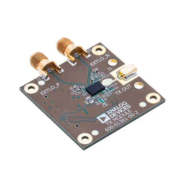
Analog Devices Inc. EV1HMC6300BG46
- Part No.:
- EV1HMC6300BG46
- Manufacturer:
- Analog Devices Inc.
- Category:
- RF, RFID, Wireless Evaluation Boards
- Package:
- Datasheet:
-
 EV1HMC6300BG46.pdf
- Description:
- HMC6300BG46 EVALUATION PCB
- Quantity:
- Payment:

- Shipping:

Inventory:2,180
Please send an inquiry. Send us your inquiry, and we will respond immediately.
Product details
Overview
EV1HMC6300BG46 from Analog Devices is a 57–64 GHz millimeter-wave transmitter IC with integrated synthesizer, 1.8 GHz modulation bandwidth, 15 dBm P1dB output power (differential), 5–35 dB gain control, and support for 256 QAM via external LO-designed for WiGig/802.11ad radio and high-definition video transmission.
For engineers reviewing the EV1HMC6300BG46 datasheet, EV1HMC6300BG46 pinout, EV1HMC6300BG46 application, or EV1HMC6300BG46 equivalent, this page delivers verified RF performance specs, WLBGA-65 package mapping, I/Q baseband interface details, and validated alternatives for 60 GHz ISM-band transceiver design.
Technical Context
The EV1HMC6300BG46 integrates a fractional-N PLL synthesizer generating 16.3–18.3 GHz LO, divided-by-2 for 8–9.1 GHz IF and tripled to 57–64 GHz RF. It supports both internal LO (250/500/540 MHz steps) and external LO injection for phase-coherent operation and 256 QAM.
Its universal analog I/Q interface accepts 5–750 mVp-p differential baseband signals with 1.6 V common-mode; digital SPI (1.2 V CMOS) and analog voltage controls manage IF/RF gain, MSK/FSK modulation, and power amplifier configuration-including single-ended/differential output selection and on-chip temperature sensing.
Key Specifications
| Parameter | Value and Actual Design Meaning |
|---|---|
| Frequency Range | 57 GHz to 64 GHz - covers full unlicensed 60 GHz ISM band including IEEE 802.11ad/WiGig channels. |
| Modulation Bandwidth | 1.8 GHz - enables multi-Gbps data rates with 256 QAM under external LO mode. |
| Output Power (P1dB) | 15 dBm differential into 100 Ω - sufficient for short-range HD video links without external PA staging. |
| Gain Control Range | 5 dB to 35 dB - digitally and analog-controllable across IF, RF, and modulator stages for dynamic range management. |
| Phase Noise | −93 dBc/Hz @ 1 MHz offset - meets spectral purity requirements for 64 QAM with internal LO. |
| Power Dissipation | 1.0 W (balanced) / 0.75 W (external LO) - thermal design must accommodate 6 mm × 4 mm WLBGA footprint. |
| Supply Voltages | VCCPAN/VCCPAP = 4.0 V; VCCDRV/VCCDIV/VCCMIX/VCCIF/VCCRFVGA/VCCTRIP/VCCVCO = 2.7 V; VDDD/VDDSYN = 1.35 V - requires seven distinct rail domains. |
| Interface | 3-wire 1.2 V CMOS serial interface - supports register-level control of PA bias, gain states, and modulation mode at >100 MHz clock rate. |
Pinout & Package
EV1HMC6300BG46 uses a 65-ball RoHS-compliant wafer-level ball grid array (WLBGA) package measuring 6 mm × 4 mm with 0.4 mm pitch. Ball assignment follows JEDEC MO-220 standard; ground balls are distributed across A–H rows for EMI suppression and thermal conduction.
| Pin/Terminal | Circuit Role | Design Meaning |
|---|---|---|
| RFOUT_P / RFOUT_N | Differential RF Output | AC-coupled 100 Ω differential port; enables linear 15 dBm output or single-ended 12 dBm when RFOUT_N is used alone. |
| BB_IP / BB_IM / BB_QP / BB_QN | Analog I/Q Baseband Inputs | DC-coupled 50 Ω inputs accepting 5–750 mVp-p, 1.6 V common-mode signals for quadrature modulation. |
| FM_PI / FM_MI / FM_PQ / FM_MQ | MSK/FSK Modulation Inputs | DC-coupled 50 Ω paths supporting low-power serial data links without high-speed DACs. |
| REFCLK_P / REFCLK_N | Differential Reference Clock Input | Accepts LVPECL/LVDS/CMOS clocks (1.2 V/2.5 V/3.3 V); determines synthesizer step size (250/500/540 MHz). |
| EXTLO_P / EXTLO_N | External LO Input | Enables user-defined LO characteristics and phase-coherent TDD/FDD operation with HMC6301 receiver. |
| DETOUT / RFB | Integrated Power Detector | Provides 0.6–2.6 V dc output proportional to RF power; requires 1.15 kΩ external resistor for P1dB coverage. |
| DATA / CLK / ENABLE | Serial Digital Interface | 1.2 V CMOS SPI-compatible bus for configuring registers, enabling/disabling blocks, and calibrating gain paths. |
| VCCPAN / VCCPAP / VCCDRV / etc. | Multi-Rail Power Supplies | 11 dedicated supply pins across 7 voltage domains ensure noise isolation between PA, mixer, synthesizer, and digital logic. |
Key Features
| Feature | Design Value |
|---|---|
| Integrated image-reject filter | 40 dBc image rejection eliminates need for external IF filtering in compact 60 GHz modules. |
| On-chip temperature sensor | Four-level output calibrated from −40°C to +85°C enables closed-loop thermal compensation without external sensors. |
| Dual LO architecture | Switchable internal synthesizer (for 64 QAM) or external LO input (for 256 QAM and phase coherence) simplifies system-level timing architecture. |
| Universal analog I/Q interface | Single baseband interface supports QAM, MSK, FSK, and OOK - reducing BOM count versus discrete modulator solutions. |
| Configurable output topology | Digital register bit (pa_se_sel) toggles between differential (15 dBm) and single-ended (12 dBm) RF output - enabling flexible PCB layout and power trade-offs. |
| Partially external loop filter | EXTFIL_P/EXTFIL_N pins allow tuning of PLL bandwidth (300 kHz typical) to balance phase noise vs. lock time for specific modulation schemes. |
Applications
| Small Cell Backhaul | WiGig/802.11ad Radio |
|---|---|
Use Scenario: Point-to-point wireless links replacing fiber in dense urban deployments with <1 km range and <10 Gbps throughput. IC Role / Device Role / Timing Role: Primary RF transmitter generating 57–64 GHz carrier with 1.8 GHz instantaneous bandwidth and 256 QAM modulation. Use Value: Integrated synthesizer and image-reject filter reduce bill-of-materials by eliminating discrete PLL, filter, and upconversion stages. |
Use Scenario: Multi-gigabit wireless docking stations and VR headset connectivity requiring ultra-low latency and high spectral efficiency. IC Role / Device Role / Timing Role: Millimeter-wave transmitter core delivering compliant 802.11ad PHY layer RF output with precise phase noise and sideband suppression. Use Value: −93 dBc/Hz phase noise @ 1 MHz offset and 30 dBc sideband suppression meet IEEE 802.11ad spectral mask requirements without post-filtering. |
| High Definition Video Transmission | Radar / High Resolution Imaging |
Use Scenario: Wireless HDMI replacement for uncompressed 4K/60fps video streaming over distances up to 10 meters in line-of-sight environments. IC Role / Device Role / Timing Role: Linear RF transmitter providing stable 15 dBm P1dB output with minimal distortion across full 57–64 GHz band. Use Value: 1.8 GHz modulation bandwidth supports >5 Gbps raw data rates required for uncompressed UHD video transport. |
Use Scenario: Short-range automotive or industrial radar systems needing fine range resolution (<5 cm) and wide field-of-view scanning. IC Role / Device Role / Timing Role: Coherent transmitter element enabling FMCW waveform generation with precise frequency ramping and low phase noise. Use Value: External LO support allows synchronization with HMC6301 receiver for true TDD coherent operation and sub-millimeter Doppler accuracy. |
Equivalent & Alternatives
The following parts are listed as comparable options for similar millimeter-wave transmitter applications.
| Alternative Part | Technical Difference | Application Difference | Selection Advice |
|---|---|---|---|
| HMC6300LP4E | Same die, leaded QFN-40 package (7 mm × 7 mm); lacks WLBGA thermal performance and RF pin layout optimization. | Better suited for prototyping and lower-frequency validation; not recommended for production 60 GHz modules requiring minimal parasitic inductance. | Select HMC6300LP4E only for lab evaluation where solder reflow compatibility and probe access outweigh RF performance needs. |
| ADAR1000 | 4-channel 24–44 GHz beamformer IC with integrated T/R switching; no internal synthesizer or baseband interface. | Targets phased-array radar, not point-to-point communication; requires external DACs, LO distribution, and IF processing. | Choose ADAR1000 for electronically steered antenna systems; EV1HMC6300BG46 remains optimal for fixed-link 60 GHz transceivers. |
Compared with HMC6300LP4E and ADAR1000, EV1HMC6300BG46 uniquely combines full 57–64 GHz transmit functionality, integrated synthesizer, analog I/Q interface, and WLBGA packaging optimized for mmWave PCB integration-making it the only drop-in solution for WiGig and 60 GHz backhaul reference designs.
Availability
EV1HMC6300BG46 is available at Aetrix Electronics and suitable for small cell backhaul, WiGig/802.11ad radio, and high-definition video transmission requiring stable component supply across extended temperature ranges and high-volume production ramps.
Supply support for EV1HMC6300BG46 includes scheduled delivery planning, volume procurement assistance, BOM continuity management, traceable sourcing, and lifecycle availability coordination for OEM customers, industrial embedded developers, connected-device designers, and electronics production programs.
Manufacturer
Analog Devices is a global leader in high-performance analog, mixed-signal, and RF ICs, serving communications, industrial, and aerospace markets with precision signal processing solutions.
The HMC6300 product line delivers fully integrated millimeter-wave transceivers for unlicensed 60 GHz ISM-band applications, targeting multi-Gbps wireless infrastructure where size, power, and spectral purity are critical constraints.
FAQ
What is the operating frequency range of the EV1HMC6300BG46?
The EV1HMC6300BG46 operates from 57 GHz to 64 GHz, covering the entire unlicensed 60 GHz ISM band. This range supports IEEE 802.11ad/WiGig channels and enables multi-Gbps data transfer for applications like wireless HD video and small cell backhaul. The device maintains specified gain, output power, and phase noise across this full band at temperatures from −40°C to +85°C.
Does the EV1HMC6300BG46 support both internal and external local oscillator modes?
Yes, the EV1HMC6300BG46 supports dual LO architectures: an integrated fractional-N synthesizer for 64 QAM (with 250/500/540 MHz step sizes) and external LO injection for 256 QAM and phase-coherent operation. When using external LO, the EV1HMC6300BG46 achieves improved phase noise floor and enables synchronized transmit/receive with the HMC6301 receiver chip in FDD or TDD configurations.
What package type does the EV1HMC6300BG46 use, and why is it significant for mmWave design?
The EV1HMC6300BG46 uses a 65-ball RoHS-compliant wafer-level ball grid array (WLBGA) package measuring 6 mm × 4 mm. Its fine-pitch (0.4 mm) and ground-ball distribution minimize parasitic inductance and thermal resistance-critical for maintaining RF integrity and power efficiency above 57 GHz. Unlike leaded alternatives, this WLBGA enables direct integration into compact mmWave modules without bond wire degradation.
How does the EV1HMC6300BG46 handle baseband interfacing for different modulation schemes?
The EV1HMC6300BG46 provides a universal analog I/Q interface (BB_IP/BB_IM/BB_QP/BB_QN) for QAM and a dedicated FSK/MSK path (FM_PI/FM_MI/FM_PQ/FM_MQ) for low-power serial links. Both accept 5–750 mVp-p differential signals with 1.6 V common-mode. Gain control is available digitally via SPI or analog voltage (0.1–2.4 V), allowing flexible integration with FPGA-based or ASIC-based baseband processors.
Can the EV1HMC6300BG46 be used in radar applications, and what features enable that?
Yes, the EV1HMC6300BG46 supports FMCW radar applications through its precise frequency synthesis, low phase noise (−93 dBc/Hz @ 1 MHz), and external LO synchronization capability. When paired with the HMC6301 receiver, the EV1HMC6300BG46 enables coherent TDD operation with sub-millimeter range resolution. Its integrated temperature sensor and detector output also support real-time calibration in varying environmental conditions.
EV1HMC6300BG46 Specifications
- Product attributes
- Attribute value
- Manufacturer:
- Analog Devices Inc.
- Series:
- -
- Packaging:
- Box
- Product Status:
- Active
- Type:
- Transmitter
- Frequency:
- 57GHz ~ 64GHz
- Contents:
- Board(s)
- Utilized IC / Part:
- HMC6300BG46
EV1HMC6300BG46 FAQ
1.How can I place an order for EV1HMC6300BG46 through Aetrix?
Please submit a Request for Quotation (RFQ) for EV1HMC6300BG46 on Aetrix. Our sales agent will provide a competitive quotation and guide you through the order confirmation once you accept the terms.
2.Are the price and stock information for EV1HMC6300BG46 reliable?
The price and inventory of EV1HMC6300BG46 are updated periodically and may fluctuate due to market conditions. Stock and pricing data are typically refreshed every 24 hours. Quotation validity for EV1HMC6300BG46 is usually 5 days.
3.What payment methods are accepted for EV1HMC6300BG46?
We accept Wire Transfer, PayPal, Credit Card, Western Union, MoneyGram, and Escrow for EV1HMC6300BG46 transactions.
Note: Certain payment methods may incur a processing fee.
4.How is shipping managed for EV1HMC6300BG46?
EV1HMC6300BG46 orders can be shipped via leading logistics carriers, including DHL, UPS, FedEx, TNT, or Registered Mail.
Once your EV1HMC6300BG46 order is processed, you will receive an email with the shipment details and tracking number.
Note: Tracking information may take up to 24 hours to appear. Express delivery typically takes 3–5 business days.
5.How can I obtain technical support or documentation for EV1HMC6300BG46?
For technical support, including EV1HMC6300BG46 datasheets, pinout diagrams, or application guidance, please contact our engineering support team. They can provide detailed documentation and assistance for your EV1HMC6300BG46 requirements.
6.How does Aetrix verify that EV1HMC6300BG46 is sourced from the original manufacturer or authorized distributors?
All EV1HMC6300BG46 products on Aetrix are procured from qualified distributors and authorized channels. Our dedicated quality assurance team conducts strict verification, including traceability checks and, if necessary, third-party testing. This ensures that EV1HMC6300BG46 meets industry standards.
7.What is the process for return or replacement of EV1HMC6300BG46?
All EV1HMC6300BG46 units undergo pre-shipment inspection (PSI). If there is an issue with EV1HMC6300BG46, returns or replacements are accepted under the following conditions:
1.Quantity discrepancies, incorrect items, or visible external defects (such as breakage or corrosion), acknowledged by Aetrix.
2.The issue is reported within 90 days of delivery.
3.The EV1HMC6300BG46 part is unused and in its original packaging.
Return procedure for EV1HMC6300BG46:
1.Submit a request within 90 days.
2.Obtain a Return Material Authorization (RMA) from Aetrix.
EV1HMC6300BG46 Tags
-
113991054
Seeed Technology Co., Ltd
-
SC0918
Raspberry Pi

-
113991114
Seeed Technology Co., Ltd
-
ESP32-C6-DEVKITM-1-N4
Espressif Systems
-
ESP32-DEVKITM-1
Espressif Systems
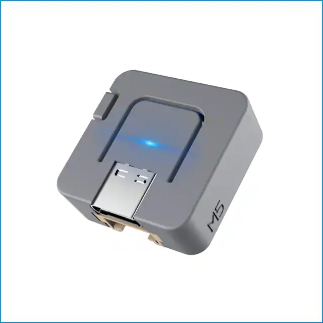
-
C008
M5Stack Technology Co., Ltd.
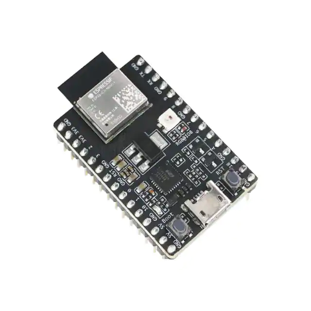
-
ESP32-C3-DEVKITC-02
Espressif Systems
-
ESP32-C6-DEVKITC-1-N8
Espressif Systems
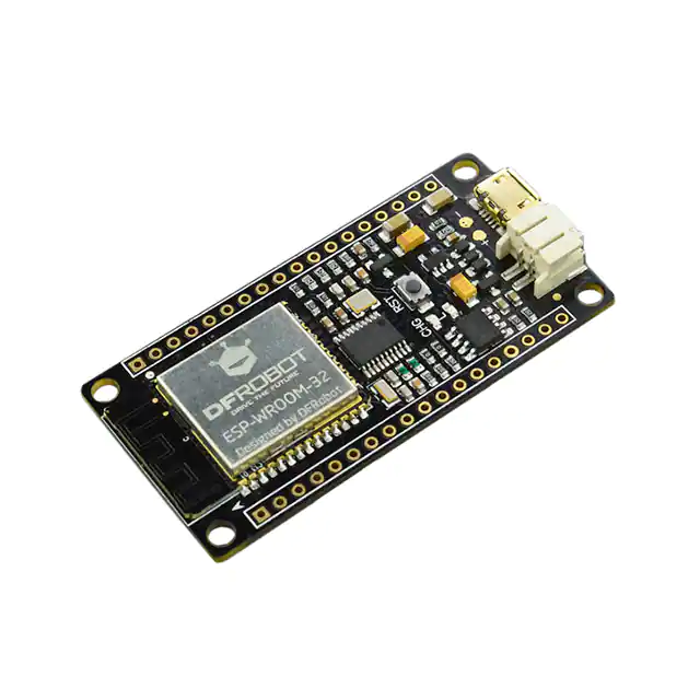
-
DFR0478
DFRobot
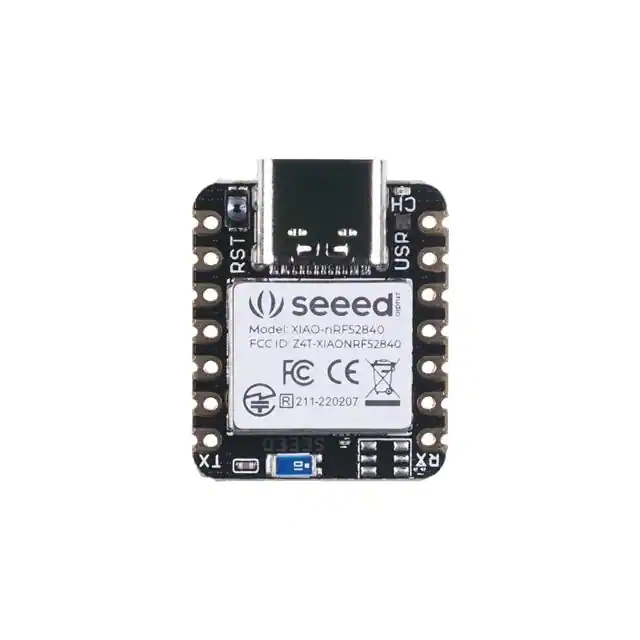
-
102010448
Seeed Technology Co., Ltd
-
ESP32-DEVKITC-32E
Espressif Systems
-
ESP32-DEVKITC-32UE
Espressif Systems
Tech Hub

A practical engineering guide to 3.3V and 5V logic compatibility, input thresholds, resistor dividers, translator ICs, MOSFET level shifting, I2C pull-ups, timing limits and power-sequencing risks.

The 74HC595 uses push-pull logic outputs, while the TPIC6B595 uses 50 V open-drain DMOS sinks for higher-power loads. This guide compares timing, current limits, 3.3 V interfacing, load wiring, thermal…

The 74HC595 converts serial data into eight stable parallel outputs. This guide covers pin functions, shift and storage timing, OE and MR behavior, drive-current limits, cascading, voltage compatibilit…

A technical comparison of level-sensitive latches and edge-triggered flip-flops, covering timing windows, setup and hold limits, master–slave operation, time borrowing, race-through, HDL inference and…

A D latch stores one bit while Enable controls when data can pass. This reference covers gate-level operation, truth tables, transparency, setup and hold timing, LE versus OE, common ICs and practical …

An SR latch stores one bit through cross-coupled feedback. This engineering reference covers NOR and NAND implementations, truth tables, forbidden-state recovery, gated operation, switch debouncing, fa…

Latch circuits retain one bit through feedback. This technical reference covers SR and D latches, truth tables, transparency, timing limits, latch-versus-flip-flop behavior, applications and common log…

An engineering guide to LED driver operation, constant-current and constant-voltage outputs, linear and switching topologies, dimming, IC selection, calculations, replacement compatibility, and fault c…

Operational amplifier guide covering op amp basics, feedback, ideal vs real op amps, common configurations, buffer circuits, offset, bias current, gain-bandwidth, slew rate, rail-to-rail limits and sel…

Jumper cables guide covering safe connection order, red and black clamp placement, final ground connection, cable gauge, length, clamp quality, copper vs CCA cables, jump starter comparison and battery…


