
 My Inquiry
 My Account


Texas Instruments FDC2112QDNTTQ1
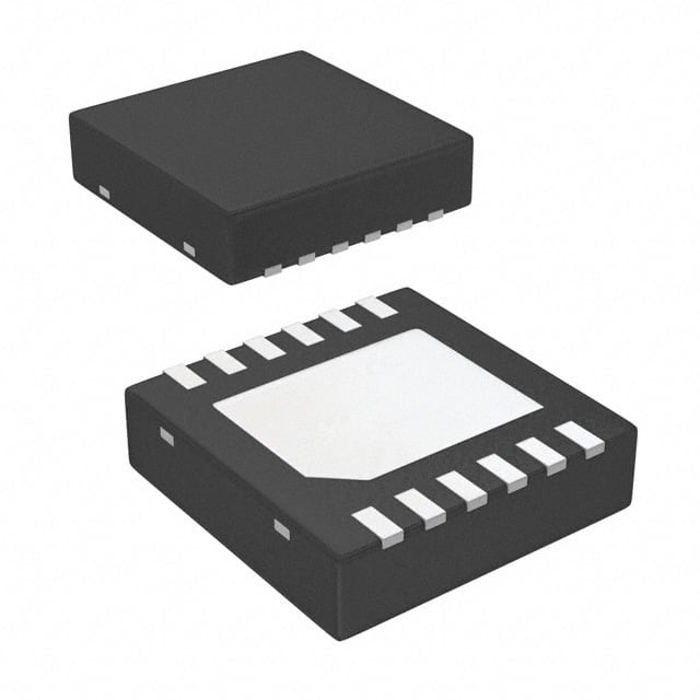
- Part No.:
- FDC2112QDNTTQ1
- Manufacturer:
- Texas Instruments
- Category:
- Sensor and Detector Interfaces
- Package:
- 12-WFDFN Exposed Pad
- Datasheet:
-
 FDC2112QDNTTQ1.pdf
- Description:
- IC FDC CAPTIVE SENSING 12WSON
- Quantity:
- Payment:

- Shipping:

Inventory:159
Please send an inquiry. Send us your inquiry, and we will respond immediately.
Product details
Overview
FDC2112QDNTTQ1 from Texas Instruments is a 2-channel, AEC-Q100 Grade 1 automotive-qualified capacitance-to-digital converter (CDC) for high-resolution capacitive sensing. It delivers up to 28-bit resolution, 13.3 kSPS maximum output rate per active channel, and 0.3 fF RMS noise at 100 SPS with 5 MHz sensor excitation - enabling precise proximity and gesture detection in harsh environments.
For engineers reviewing the FDC2112QDNTTQ1 datasheet, FDC2112QDNTTQ1 pinout, FDC2112QDNTTQ1 application, or FDC2112QDNTTQ1 equivalent, key selection criteria include its resonant L-C tank architecture, I²C interface, 2.7–3.6 V supply, –40°C to +125°C operation, and WSON-12 (4 mm × 4 mm) package with integrated ground DAP.
Technical Context
The FDC2112QDNTTQ1 employs a narrow-band resonant sensing architecture that measures sensor capacitance via frequency shift of an external L-C tank, not switched-capacitor sampling. Its core digitizes the ratio fSENSOR/fREF, where fREF is derived from either an internal 43.4 MHz oscillator or an external clock (2–40 MHz).
It supports programmable sensor excitation (10 kHz–10 MHz), configurable settling time per channel, and dual-channel sequential conversion. The device uses differential input pairs (IN0A/IN0B, IN1A/IN1B) to reject common-mode noise and includes EMI-resistant design validated under AEC-Q100 HBM ±2 kV and CDM ±750 V.
Key Specifications
| Parameter | Value and Actual Design Meaning |
|---|---|
| Resolution | Up to 28 bits - enables sub-femtofarad capacitance change detection for ultra-sensitive touch/proximity systems. |
| Max sample rate | 13.3 kSPS (single channel) - supports real-time gesture recognition with low latency. |
| RMS noise | 0.3 fF at 100 SPS / 5 MHz fSENSOR - ensures stable measurements in noisy automotive cabin environments. |
| Supply voltage | 2.7 V to 3.6 V - compatible with standard 3.3 V automotive power rails and low-voltage microcontrollers. |
| Operating temp | –40°C to +125°C ambient - meets AEC-Q100 Grade 1 requirements for under-hood and door module placement. |
| Interface | I²C (up to 400 kHz) - simplifies host MCU integration with minimal pin count and no need for SPI or custom timing logic. |
| Power modes | 2.1 mA active, 35 µA sleep, 200 nA shutdown - enables battery-conscious designs in always-on proximity sensors. |
Pinout & Package
The FDC2112QDNTTQ1 is housed in a 12-pin WSON (DNT) package measuring 4 mm × 4 mm with an exposed die attach pad (DAP) that must be connected to ground for optimal thermal and EMI performance.
| Pin/Terminal | Circuit Role | Design Meaning |
|---|---|---|
| SCL | I²C clock input | Drives synchronous communication; requires external pull-up to VDD (3.3 V typical). |
| SDA | I²C bidirectional data line | Carries configuration writes and 28-bit channel data reads; open-drain, requires pull-up. |
| CLKIN | External controller clock input | Accepts 2–40 MHz clock; tie to GND to enable internal 43.4 MHz oscillator. |
| ADDR | I²C address select | Logic level sets I²C address: ADDR = LOW → 0x2A; ADDR = HIGH → 0x2B. |
| INTB | Configurable interrupt output | Active-low open-drain signal indicating data ready, error, or threshold crossing. |
| SD | Shutdown control input | High = normal operation; low = 200 nA shutdown mode (asynchronous entry/exit). |
| VDD | Power supply | 2.7–3.6 V analog/digital supply; decoupling capacitor (0.1 µF + 1 µF) required near pin. |
| GND | Ground reference | Analog/digital ground; must be connected to PCB ground plane and DAP. |
| IN0A / IN0B | Differential sensor inputs ch0 | Connect to opposite ends of LC tank; rejects common-mode EMI and cable noise. |
| IN1A / IN1B | Differential sensor inputs ch1 | Second independent LC sensing channel; supports temperature-compensated dual-sensor layouts. |
| DAP | Exposed thermal pad | Internally tied to GND; solder to solid ground plane for thermal dissipation and noise immunity. |
Key Features
| Feature | Design Value |
|---|---|
| L-C resonant architecture | Measures capacitance via frequency shift of external LC tank - immune to LED/fluorescent light interference and board-level EMI. |
| AEC-Q100 Grade 1 qualification | Validated for –40°C to +125°C operation, HBM ±2 kV, CDM ±750 V - suitable for automotive door, kick, and console sensors. |
| Programmable excitation range | 10 kHz to 10 MHz sensor drive frequency - allows optimization for sensor size, material, and environmental coupling. |
| Dual-channel sequential conversion | Automatically cycles between two channels with configurable dwell time - enables reference-sensor drift cancellation. |
| Low-power operation modes | 2.1 mA active, 35 µA sleep, 200 nA shutdown - extends battery life in wireless or energy-harvested proximity nodes. |
Applications
| Proximity Sensing | Gesture Recognition |
|---|---|
Use Scenario: Detect hand presence near vehicle door handle without physical contact. IC Role / Device Role / Timing Role: Converts minute capacitance shifts from human body proximity into high-resolution digital values using differential L-C tank sensing. Use Value: Enables reliable wake-up of door lock system with <0.3 fF noise floor and immunity to ambient lighting interference. | Use Scenario: Recognize swipe or hover gestures above center console for HVAC or infotainment control. IC Role / Device Role / Timing Role: Samples two independent sensor channels at 13.3 kSPS to track dynamic capacitance gradients across spatial array. Use Value: Delivers sub-10-ms response latency and 28-bit resolution for robust multi-gesture classification in cockpit environments. |
| Automotive Door Sensors | Conductive Liquid Level Sensing |
Use Scenario: Trigger passive entry system when user's foot approaches rear bumper (kick-to-open). IC Role / Device Role / Timing Role: Acts as dedicated CDC for ruggedized metal-encapsulated LC sensor mounted in bumper fascia. Use Value: Maintains accuracy across –40°C to +125°C with AEC-Q100 validated thermal stability and ESD hardening. | Use Scenario: Monitor fuel or washer fluid level in plastic tank using conductive probe electrodes. IC Role / Device Role / Timing Role: Measures capacitance change between parallel electrodes immersed in liquid, rejecting parasitic tank-wall coupling. Use Value: Supports up to 250 nF sensor capacitance with 1 mH inductor, enabling long probe lengths and large-volume tanks. |
Equivalent & Alternatives
The following parts are listed as comparable options for similar capacitance-to-digital conversion applications.
| Alternative Part | Technical Difference | Application Difference | Selection Advice |
|---|---|---|---|
| FDC2114QDSGRQ1 | 4-channel variant in 16-pin WQFN; identical resolution, noise, and architecture but adds two extra differential input pairs. | Required for systems needing >2 independent sensing zones (e.g., multi-zone door handle or panoramic gesture panel). | Select FDC2114QDSGRQ1 only if additional channels justify larger footprint and routing complexity. |
| FDC2212QDNTTQ1 | Same 2-channel WSON-12 package but with 28-bit resolution enabled by default (FDC2112 supports 12- or 28-bit via register config); higher RMS noise (0.8 fF) at same conditions. | Better suited for cost-sensitive applications where 28-bit resolution is mandatory and 0.3 fF noise is not required. | FDC2212QDNTTQ1 offers guaranteed 28-bit output but trades off noise performance; verify SNR budget before substitution. |
Compared with FDC2112QDNTTQ1, the FDC2114QDSGRQ1 adds two channels in a larger package for expanded sensing coverage, while the FDC2212QDNTTQ1 guarantees full 28-bit output at the expense of higher noise - making FDC2112QDNTTQ1 optimal for high-SNR, dual-zone automotive proximity systems.
Availability
FDC2112QDNTTQ1 is available at Aetrix Electronics and suitable for automotive proximity sensing, gesture interface, and conductive liquid level monitoring requiring stable component supply across extended temperature ranges and long production lifecycles.
Supply support for FDC2112QDNTTQ1 includes scheduled delivery planning, volume procurement assistance, BOM continuity management, traceable sourcing, and lifecycle availability coordination for OEM customers, industrial embedded developers, connected-device designers, and electronics production programs.
Manufacturer
Texas Instruments is a global semiconductor leader specializing in analog, embedded processing, and automotive ICs, with decades of expertise in precision sensing and automotive-grade reliability.
The FDC2x1x-Q1 product line was designed specifically for robust, high-resolution capacitive sensing in automotive interiors and exteriors - addressing EMI resilience, temperature drift, and functional safety requirements from the silicon level.
FAQ
What is the maximum sensor capacitance supported by the FDC2112QDNTTQ1?
The FDC2112QDNTTQ1 supports up to 250 nF maximum sensor capacitance when paired with a 1 mH inductor at 10 kHz oscillation frequency. This specification is measured under defined test conditions and enables use with large-area or long-probe capacitive sensors in automotive and industrial applications. Exceeding this value may reduce measurement stability or dynamic range. The FDC2112QDNTTQ1 achieves this via its resonant L-C tank architecture, which differs fundamentally from switched-capacitor CDCs.
Does the FDC2112QDNTTQ1 require an external crystal or oscillator?
No, the FDC2112QDNTTQ1 does not require an external crystal. It integrates a factory-trimmed 43.4 MHz internal oscillator usable as the controller clock source (fCLK). Alternatively, an external clock (2–40 MHz) can be applied to CLKIN for higher precision. When using the internal oscillator, CLKIN must be tied to GND. The FDC2112QDNTTQ1's clocking architecture allows flexible trade-offs between cost, board space, and timing accuracy depending on system requirements.
How many capacitive sensing channels does the FDC2112QDNTTQ1 provide?
The FDC2112QDNTTQ1 provides two fully independent capacitive sensing channels, each with differential input pairs (IN0A/IN0B and IN1A/IN1B). Both channels support programmable excitation frequency, settling time, and reference clock division. The device operates in either single-channel mode (one channel continuously sampled) or dual-channel auto-scan mode (sequentially cycling between both), enabling temperature drift compensation using one channel as a reference. This matches the "2112" designation in the FDC2112QDNTTQ1 part number.
What package type and dimensions does the FDC2112QDNTTQ1 use?
The FDC2112QDNTTQ1 uses a 12-pin WSON package (Texas Instruments designation: DNT), with nominal dimensions of 4 mm × 4 mm and an exposed die attach pad (DAP) on the bottom. The DAP must be soldered to a PCB ground plane for thermal management and EMI suppression. Pin pitch is 0.5 mm. This compact, leadless package supports high-density automotive PCB layouts while maintaining AEC-Q100 thermal and mechanical robustness - confirmed by RθJA = 36.7°C/W and qualified operation from –40°C to +125°C.
Is the FDC2112QDNTTQ1 qualified for automotive applications?
Yes, the FDC2112QDNTTQ1 is explicitly qualified for automotive applications under AEC-Q100 with Grade 1 temperature rating (–40°C to +125°C ambient), HBM ESD level 2 (±2 kV), and CDM level C5 (±750 V). It is manufactured and tested to meet stringent automotive reliability, traceability, and process control standards. The "Q1" suffix in FDC2112QDNTTQ1 denotes this automotive qualification, distinguishing it from commercial-grade variants. All electrical, thermal, and stress test data in the official datasheet reflect AEC-Q100-compliant characterization.
FDC2112QDNTTQ1 Specifications
- Product attributes
- Attribute value
- Manufacturer:
- Texas Instruments
- Package/Case:
- 12-WFDFN Exposed Pad
- Series:
- -
- Packaging:
- Tape & Reel (TR)
- Product Status:
- Obsolete
- Programmable:
- Not Verified
- Type:
- Interface
- Input Type:
- Capacitive
- Output Type:
- I2C
- Current - Supply:
- 2.1 mA
- Operating Temperature:
- -40°C ~ 125°C
- Grade:
- Automotive
- Qualification:
- AEC-Q100
- Mounting Type:
- Surface Mount
- Supplier Device Package:
- 12-WSON (4x4)
FDC2112QDNTTQ1 FAQ
1.How can I place an order for FDC2112QDNTTQ1 through Aetrix?
Please submit a Request for Quotation (RFQ) for FDC2112QDNTTQ1 on Aetrix. Our sales agent will provide a competitive quotation and guide you through the order confirmation once you accept the terms.
2.Are the price and stock information for FDC2112QDNTTQ1 reliable?
The price and inventory of FDC2112QDNTTQ1 are updated periodically and may fluctuate due to market conditions. Stock and pricing data are typically refreshed every 24 hours. Quotation validity for FDC2112QDNTTQ1 is usually 5 days.
3.What payment methods are accepted for FDC2112QDNTTQ1?
We accept Wire Transfer, PayPal, Credit Card, Western Union, MoneyGram, and Escrow for FDC2112QDNTTQ1 transactions.
Note: Certain payment methods may incur a processing fee.
4.How is shipping managed for FDC2112QDNTTQ1?
FDC2112QDNTTQ1 orders can be shipped via leading logistics carriers, including DHL, UPS, FedEx, TNT, or Registered Mail.
Once your FDC2112QDNTTQ1 order is processed, you will receive an email with the shipment details and tracking number.
Note: Tracking information may take up to 24 hours to appear. Express delivery typically takes 3–5 business days.
5.How can I obtain technical support or documentation for FDC2112QDNTTQ1?
For technical support, including FDC2112QDNTTQ1 datasheets, pinout diagrams, or application guidance, please contact our engineering support team. They can provide detailed documentation and assistance for your FDC2112QDNTTQ1 requirements.
6.How does Aetrix verify that FDC2112QDNTTQ1 is sourced from the original manufacturer or authorized distributors?
All FDC2112QDNTTQ1 products on Aetrix are procured from qualified distributors and authorized channels. Our dedicated quality assurance team conducts strict verification, including traceability checks and, if necessary, third-party testing. This ensures that FDC2112QDNTTQ1 meets industry standards.
7.What is the process for return or replacement of FDC2112QDNTTQ1?
All FDC2112QDNTTQ1 units undergo pre-shipment inspection (PSI). If there is an issue with FDC2112QDNTTQ1, returns or replacements are accepted under the following conditions:
1.Quantity discrepancies, incorrect items, or visible external defects (such as breakage or corrosion), acknowledged by Aetrix.
2.The issue is reported within 90 days of delivery.
3.The FDC2112QDNTTQ1 part is unused and in its original packaging.
Return procedure for FDC2112QDNTTQ1:
1.Submit a request within 90 days.
2.Obtain a Return Material Authorization (RMA) from Aetrix.
FDC2112QDNTTQ1 Tags

-
RE46C100S8TF
Microchip Technology

-
XTR111AIDRCR
Texas Instruments

-
XTR111AIDGQR
Texas Instruments

-
XTR117AIDGKR
Texas Instruments
-
XTR111AIDGQT
Texas Instruments

-
XTR115UA/2K5
Texas Instruments
-
MAX14626ETT+T
Analog Devices Inc./Maxim Integrated
-
XTR116UA/2K5
Texas Instruments
-
XTR115U/2K5
Texas Instruments
-
XTR116U/2K5
Texas Instruments

-
PGA308AIDGSR
Texas Instruments
-
XTR300AIRGWR
Texas Instruments
Tech Hub

A practical engineering guide to 3.3V and 5V logic compatibility, input thresholds, resistor dividers, translator ICs, MOSFET level shifting, I2C pull-ups, timing limits and power-sequencing risks.

The 74HC595 uses push-pull logic outputs, while the TPIC6B595 uses 50 V open-drain DMOS sinks for higher-power loads. This guide compares timing, current limits, 3.3 V interfacing, load wiring, thermal…

The 74HC595 converts serial data into eight stable parallel outputs. This guide covers pin functions, shift and storage timing, OE and MR behavior, drive-current limits, cascading, voltage compatibilit…

A technical comparison of level-sensitive latches and edge-triggered flip-flops, covering timing windows, setup and hold limits, master–slave operation, time borrowing, race-through, HDL inference and…

A D latch stores one bit while Enable controls when data can pass. This reference covers gate-level operation, truth tables, transparency, setup and hold timing, LE versus OE, common ICs and practical …

An SR latch stores one bit through cross-coupled feedback. This engineering reference covers NOR and NAND implementations, truth tables, forbidden-state recovery, gated operation, switch debouncing, fa…

Latch circuits retain one bit through feedback. This technical reference covers SR and D latches, truth tables, transparency, timing limits, latch-versus-flip-flop behavior, applications and common log…

An engineering guide to LED driver operation, constant-current and constant-voltage outputs, linear and switching topologies, dimming, IC selection, calculations, replacement compatibility, and fault c…

Operational amplifier guide covering op amp basics, feedback, ideal vs real op amps, common configurations, buffer circuits, offset, bias current, gain-bandwidth, slew rate, rail-to-rail limits and sel…

Jumper cables guide covering safe connection order, red and black clamp placement, final ground connection, cable gauge, length, clamp quality, copper vs CCA cables, jump starter comparison and battery…


