
 My Inquiry
 My Account


onsemi FUSB301TMX
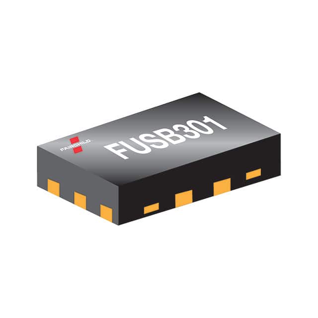
- Part No.:
- FUSB301TMX
- Manufacturer:
- onsemi
- Category:
- Controllers
- Package:
- 10-XFQFN
- Datasheet:
-
 FUSB301TMX.pdf
- Description:
- IC CONTROLLER USB 10TMLP
- Quantity:
- Payment:

- Shipping:

Inventory:6,035
Please send an inquiry. Send us your inquiry, and we will respond immediately.
Product details
Overview
FUSB301TMX from onsemi is a fully autonomous USB Type-C controller optimized for <15 W applications, implementing CC logic detection for Source, Sink, and Dual Role Port (DRP) modes, supporting dead battery operation and external SuperSpeed switch control via the SS_SW pin. It operates from 3.0 V to 5.5 V, consumes ≤2 µA in disable mode, and is housed in a 10-lead TMLP package (1.6 mm × 1.2 mm × 0.375 mm).
For engineers reviewing the FUSB301TMX datasheet, pinout, applications, or equivalent options, key selection criteria include autonomous DRP timing control, I²C slave interface (400 kHz fast mode), CC line debounce timing (75 ms sink / 150 ms source), dead battery pull-down capability (≤2.18 V), and SS_SW truth-table–driven USB 3.1 Gen 1 switch coordination.
Technical Context
The FUSB301TMX integrates a state machine that autonomously manages USB Type-C attachment/detachment, orientation detection (ORIENT[1:0]), and current advertisement level decoding (BC_LVL[1:0]) without host processor intervention. Its CC detection circuitry supports Ra/Rd thresholds per USB Type-C spec v1.1: 0.20 V (Ra), 1.60 V (Rd default), and 2.60 V (Rd 3 A).
It features an open-drain INT_N interrupt output with configurable mask register (INT_MASK), a CMOS SS_SW output synchronized to CC orientation (ORIENT1/ORIENT0), and I²C slave interface with fixed 0x4A address. The device supports DRP toggle timing (20–70 ms) via DRPTOGGLE bits and enables dead battery operation by activating internal Rd pull-down when VDD = 0 V and CC is pulled up by a source.
Key Specifications
| Parameter | Value and Actual Design Meaning |
|---|---|
| VDD Range | 3.0 V to 5.5 V - Supports direct connection to system VIO or PMIC rails without LDO |
| Disable Current | ≤2 µA - Enables ultra-low-power system suspend states with no wake-up latency penalty |
| CC Debounce (Sink) | 75 ms typical - Prevents false attach/detach events during cable flex or contact bounce |
| Rd Pull-Down | 5.1 kΩ typical - Matches USB Type-C spec Rd tolerance for reliable sink detection |
| I²C Speed | 400 kHz fast mode - Allows efficient register access without slowing host firmware execution |
| SS_SW Logic | CMOS output with ORIENT-driven truth table - Directly controls FUSB340-type USB 3.1 switches without GPIO polling |
| ESD Protection | 2 kV HBM on CC/VBUS - Meets IEC 61000-4-2 system-level ESD robustness for consumer ports |
Pinout & Package
Package: 10-lead ultra-thin molded leadless package (TMLP), 1.6 mm × 1.2 mm × 0.375 mm, X2QFN-10 (Case 722AC).
| Pin/Terminal | Circuit Role | Design Meaning |
|---|---|---|
| CC1, CC2 | Type-C Configuration Channel I/O | Dual bidirectional pins for detecting cable orientation, source/sink role, and accessory type per USB Type-C spec |
| VBUS | Input | Detects presence/absence of VBUS (3.7–21 V) to trigger attach/detach interrupts and enable dead battery mode |
| GND | Ground | Reference for all analog comparators and digital logic; must be low-impedance return path for CC sensing |
| VDD | Power | Supplies internal regulator and logic; powers CC comparators and I²C interface |
| SDA, SCL | I²C Slave Interface | Fast-mode (400 kHz) serial bus for configuration, status readback, and interrupt handling |
| ID | Open-drain Output | Signals sink detection to host processor's USB 2.0 input; Hi-Z when not asserted |
| SS_SW | CMOS Output | Drives external USB 3.1 Gen 1 switch (e.g., FUSB340) based on ORIENT[1:0] state-no software polling required |
| INT_N | Open-drain Interrupt | Active-low signal alerts host processor of attach/detach/accessory events; requires external pull-up |
Key Features
| Feature | Design Value |
|---|---|
| Autonomous DRP Toggle | Configurable 20–70 ms unattached state timing eliminates need for host timer management |
| Dead Battery Support | Enables sink functionality with 0 V VDD by using CC line power-critical for smartphones left discharged |
| SuperSpeed Switch Control | SS_SW pin outputs orientation-correct logic per Table 1, enabling seamless USB 3.1 Gen 1 data path routing |
| Accessory Detection | Distinguishes Audio Accessory (0x01) and Debug Accessory (0x02) in TYPE register for OS-level driver selection |
| I²C Register Map | 16-bit address space with dedicated STATUS (0x11), TYPE (0x12), and INTERRUPT (0x13) registers for deterministic event handling |
Applications
| Smartphone Charging Port | Tablet DRP Interface |
|---|---|
Use Scenario: USB-C port on mid-tier smartphone supporting charging, data transfer, and audio accessory detection. IC Role / Device Role / Timing Role: Autonomous Type-C controller managing role negotiation, VBUS monitoring, and SS_SW–driven USB 3.1 switch routing. Use Value: Eliminates need for dedicated MCU GPIOs and firmware state machine-reduces BOM cost and firmware development time. | Use Scenario: Dual-role USB-C port on Android tablet enabling host/peripheral mode switching and DisplayPort Alt Mode readiness. IC Role / Device Role / Timing Role: DRP controller with 25 ms toggle timing (DRPTOGGLE=10) and BC_LVL–based current advertisement decoding. Use Value: Ensures sub-100 ms role transition while maintaining compliance with USB Type-C v1.1 Rd threshold requirements (1.60 V ±0.05 V). |
| Notebook Docking Interface | Ultra-Portable Power Bank |
Use Scenario: USB-C docking station port negotiating power delivery, data, and video with laptop while detecting debug accessories. IC Role / Device Role / Timing Role: Source-mode controller with 330 µA HOST_CUR1/0=11 pull-up, ID pin signaling sink detection to host SoC. Use Value: Delivers 3 A sourcing capability with validated Ra detection (0.20 V) and I²C-configurable interrupt masking for clean system integration. | Use Scenario: Compact power bank with USB-C input/output supporting dead battery charging and accessory detection. IC Role / Device Role / Timing Role: Sink-mode controller enabling VBUS detection at 3.7 V threshold and automatic Rd activation when VDD = 0 V. Use Value: Guarantees reliable charging initiation even when power bank battery is fully depleted-no manual reset required. |
Equivalent & Alternatives
The following parts are listed as comparable options for similar USB Type-C controller applications.
| Alternative Part | Technical Difference | Application Difference | Selection Advice |
|---|---|---|---|
| TUSB320LAR | Supports USB PD communication via BMC PHY; lacks SS_SW pin and dead battery Rd activation | Required for USB PD 2.0/3.0 negotiation; unsuitable for pure Type-C DRP without PD | Select when PD messaging is mandatory; avoid if only basic Type-C role control and SS switch coordination are needed |
| IP5306 | Integrated Li-ion charger + Type-C controller; no I²C interface; fixed 5 V output only | Targeted at single-cell power banks; no support for DRP toggle timing or accessory detection | Select for cost-sensitive, fixed-function power banks; avoid for host-controlled DRP or multi-role systems |
Compared with TUSB320LAR and IP5306, the FUSB301TMX uniquely combines autonomous DRP timing, SS_SW–driven USB 3.1 switch control, and true dead battery operation-making it optimal for compact, low-power consumer devices where PD negotiation is unnecessary but robust Type-C interoperability is critical.
Availability
FUSB301TMX is available at Aetrix Electronics and suitable for smartphone charging ports, tablet DRP interfaces, notebook docking stations, ultra-portable power banks, and USB-C accessory detection systems requiring stable component supply across industrial temperature ranges (−40°C to +85°C).
Supply support for FUSB301TMX includes scheduled delivery planning, volume procurement assistance, BOM continuity management, traceable sourcing, and lifecycle availability coordination for OEM customers, industrial embedded developers, connected-device designers, and electronics production programs.
Manufacturer
onsemi is a global semiconductor supplier delivering energy-efficient, intelligent power and sensing solutions for automotive, industrial, cloud, medical, and IoT applications.
The FUSB301TMX belongs to onsemi's USB Type-C interface product line, designed specifically for autonomous, low-power, and space-constrained USB-C implementations in consumer portable electronics.
FAQ
What is the primary function of the FUSB301TMX in a USB-C system?
The FUSB301TMX serves as a fully autonomous USB Type-C controller responsible for CC line detection, role determination (Source/Sink/DRP), orientation identification, VBUS monitoring, and external SuperSpeed switch control. It operates independently of the host processor for core Type-C state transitions, reducing firmware overhead and enabling faster, more reliable port negotiation in devices like smartphones and tablets.
Does the FUSB301TMX support USB Power Delivery (PD) protocol negotiation?
No, the FUSB301TMX does not support USB Power Delivery (PD) protocol negotiation. It implements only the USB Type-C specification v1.0/v1.1 for role detection, orientation, and current advertisement (default/1.5 A/3 A). For PD communication-including variable voltage negotiation and structured VDMs-a separate PD controller (e.g., FUSB302B or TUSB320) is required alongside the FUSB301TMX.
How does the FUSB301TMX handle dead battery scenarios?
When VDD = 0 V and the FUSB301TMX is connected to a powered USB-C source, the source pulls up the CC line. The FUSB301TMX detects this condition and activates its internal 5.1 kΩ Rd pull-down resistor, bringing the CC voltage into the valid sink detection range (≤2.18 V). This triggers the source to enable VBUS, allowing the host system to power up and begin normal operation-enabling "dead battery" charging without external circuitry.
What is the purpose of the SS_SW pin on the FUSB301TMX?
The SS_SW pin is a CMOS output that autonomously controls an external USB 3.1 Gen 1 SuperSpeed switch (e.g., FUSB340) based on real-time CC orientation detection (ORIENT1/ORIENT0). It eliminates the need for host processor polling or GPIO toggling, ensuring correct high-speed data path routing regardless of cable flip-critical for seamless USB 3.1 operation in compact portable designs.
Can the FUSB301TMX be used in both Source and Sink modes simultaneously?
No, the FUSB301TMX cannot operate in Source and Sink modes simultaneously. It supports Dual Role Port (DRP) mode, which alternates between Unattached.Sink and Unattached.Source states using configurable toggle timing (20–70 ms). During active attachment, it assumes a single defined role (Source or Sink) based on CC line detection and MODES register configuration-consistent with USB Type-C specification behavior.
FUSB301TMX Specifications
- Product attributes
- Attribute value
- Manufacturer:
- onsemi
- Package/Case:
- 10-XFQFN
- Programmable:
- Not Verified
- Protocol:
- USB
- Function:
- Controller
- Interface:
- I2C, USB
- Standards:
- USB 2.0
- Voltage - Supply:
- 2.8V ~ 5.5V
- Current - Supply:
- 356µA
- Operating Temperature:
- -40°C ~ 85°C (TA)
- Supplier Device Package:
- 10-X2QFN (1.6x1.2)
- Grade:
- -
- Qualification:
- -
FUSB301TMX FAQ
1.How can I place an order for FUSB301TMX through Aetrix?
Please submit a Request for Quotation (RFQ) for FUSB301TMX on Aetrix. Our sales agent will provide a competitive quotation and guide you through the order confirmation once you accept the terms.
2.Are the price and stock information for FUSB301TMX reliable?
The price and inventory of FUSB301TMX are updated periodically and may fluctuate due to market conditions. Stock and pricing data are typically refreshed every 24 hours. Quotation validity for FUSB301TMX is usually 5 days.
3.What payment methods are accepted for FUSB301TMX?
We accept Wire Transfer, PayPal, Credit Card, Western Union, MoneyGram, and Escrow for FUSB301TMX transactions.
Note: Certain payment methods may incur a processing fee.
4.How is shipping managed for FUSB301TMX?
FUSB301TMX orders can be shipped via leading logistics carriers, including DHL, UPS, FedEx, TNT, or Registered Mail.
Once your FUSB301TMX order is processed, you will receive an email with the shipment details and tracking number.
Note: Tracking information may take up to 24 hours to appear. Express delivery typically takes 3–5 business days.
5.How can I obtain technical support or documentation for FUSB301TMX?
For technical support, including FUSB301TMX datasheets, pinout diagrams, or application guidance, please contact our engineering support team. They can provide detailed documentation and assistance for your FUSB301TMX requirements.
6.How does Aetrix verify that FUSB301TMX is sourced from the original manufacturer or authorized distributors?
All FUSB301TMX products on Aetrix are procured from qualified distributors and authorized channels. Our dedicated quality assurance team conducts strict verification, including traceability checks and, if necessary, third-party testing. This ensures that FUSB301TMX meets industry standards.
7.What is the process for return or replacement of FUSB301TMX?
All FUSB301TMX units undergo pre-shipment inspection (PSI). If there is an issue with FUSB301TMX, returns or replacements are accepted under the following conditions:
1.Quantity discrepancies, incorrect items, or visible external defects (such as breakage or corrosion), acknowledged by Aetrix.
2.The issue is reported within 90 days of delivery.
3.The FUSB301TMX part is unused and in its original packaging.
Return procedure for FUSB301TMX:
1.Submit a request within 90 days.
2.Obtain a Return Material Authorization (RMA) from Aetrix.
FUSB301TMX Tags

-
PTN5150AHXMP
NXP Semiconductors

-
USB3740B-AI9-TR
Microchip Technology

-
USB3740B-AI2-TR
Microchip Technology

-
USB3300-EZK-TR
Microchip Technology
-
USB3300-EZK
Microchip Technology

-
FUSB340TMX
onsemi

-
FUSB302BMPX
onsemi

-
DP83826IRHBR
Texas Instruments

-
MCP2518FDT-E/QBB
Microchip Technology
-
FUSB302MPX
onsemi

-
MCP2518FDT-E/SL
Microchip Technology

-
FT260Q-R
FTDI, Future Technology Devices International Ltd
Tech Hub

Counterfeit components can hide behind convincing markings and passing basic function tests. This engineering reference covers source traceability, external inspection, X-ray, XRF, electrical testing, …

A practical engineering and sourcing framework covering lifecycle verification, lifetime-buy calculations, replacement qualification, supplier checks and counterfeit-risk controls.

TTL and CMOS logic families differ in thresholds, loading, output drive, power and timing. This engineering guide compares 74HC and 74HCT, calculates noise margins and checks 3.3 V/5 V compatibility.

A practical engineering guide to 3.3V and 5V logic compatibility, input thresholds, resistor dividers, translator ICs, MOSFET level shifting, I2C pull-ups, timing limits and power-sequencing risks.

The 74HC595 uses push-pull logic outputs, while the TPIC6B595 uses 50 V open-drain DMOS sinks for higher-power loads. This guide compares timing, current limits, 3.3 V interfacing, load wiring, thermal…

The 74HC595 converts serial data into eight stable parallel outputs. This guide covers pin functions, shift and storage timing, OE and MR behavior, drive-current limits, cascading, voltage compatibilit…

A technical comparison of level-sensitive latches and edge-triggered flip-flops, covering timing windows, setup and hold limits, master–slave operation, time borrowing, race-through, HDL inference and…

A D latch stores one bit while Enable controls when data can pass. This reference covers gate-level operation, truth tables, transparency, setup and hold timing, LE versus OE, common ICs and practical …

An SR latch stores one bit through cross-coupled feedback. This engineering reference covers NOR and NAND implementations, truth tables, forbidden-state recovery, gated operation, switch debouncing, fa…

Latch circuits retain one bit through feedback. This technical reference covers SR and D latches, truth tables, transparency, timing limits, latch-versus-flip-flop behavior, applications and common log…


