
 My Inquiry
 My Account


onsemi FUSB307BVMPX
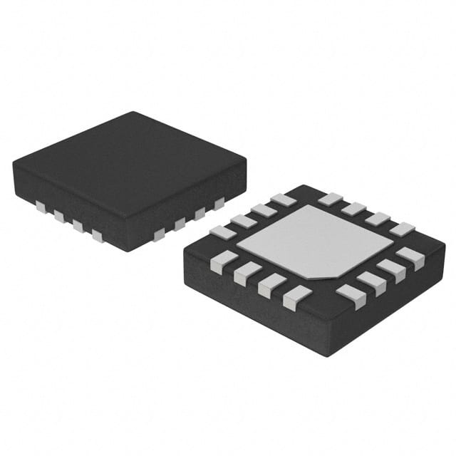
- Part No.:
- FUSB307BVMPX
- Manufacturer:
- onsemi
- Category:
- Controllers
- Package:
- 16-WFQFN Exposed Pad
- Datasheet:
-
 FUSB307BVMPX.pdf
- Description:
- IC USB CONTROLLER I2C 16WQFN
- Quantity:
- Payment:

- Shipping:

Inventory:13,583
Please send an inquiry. Send us your inquiry, and we will respond immediately.
Product details
Overview
FUSB307BVMPX from onsemi is an automotive-grade USB Type-C Port Controller (TCPC) with integrated USB Power Delivery (PD) Rev 3.0 Ver 1.1 support, 10-bit VBUS ADC, and dual-role port (DRP) functionality. It autonomously handles BMC PD packet transmission/reception, GoodCRC response, and VBUS source/sink control via dedicated SNK/SRC outputs. Designed for dead-battery operation, it powers TCPMs from VBUS and delivers regulated 3.3 V via its internal LDO.
For engineers reviewing the FUSB307BVMPX datasheet, pinout, applications, or equivalent options, key selection considerations include its −40°C to +105°C automotive temperature rating, QFN-16 package with CC1/CC2/INT_N/SCL1/SDA1 interface signals, VCONN switching capability, and I²C-addressable configuration supporting four slave addresses.
Technical Context
The FUSB307BVMPX implements a full BMC physical layer with autonomous transmit/receive state machines, automatic GoodCRC generation for valid SOP* messages, and hardware-accelerated Hard Reset/Cable Reset signaling. Its Type-C Rev 1.3 detection circuitry supports manual attach/detach sensing and orientation detection via ORIENT pin.
It integrates VBUS monitoring (10-bit ADC), programmable VCONN current limiting (210.5 mA default or configurable), and dual GPIOs configurable as CMOS I/O or open-drain outputs. Power management includes dead-battery startup from VBUS, LDO bypass at VDDGOOD threshold, and auto-discharge control for both source and sink paths.
Key Specifications
| Parameter | Value and Actual Design Meaning |
|---|---|
| USB-PD Compliance | USB-PD Rev 3.0 Ver 1.1 and Interface Spec Rev 1.0 Ver 1.2 - enables standardized communication with TCPM for contract negotiation and role swap. |
| Type-C Compliance | USB Type-C Rev 1.3 - supports full connector detection, orientation sensing, and debug accessory identification without host intervention. |
| Operating Temp | −40°C to +105°C - qualified for automotive cabin and infotainment applications per AEC-Q100 stress requirements. |
| VBUS Monitoring | 10-bit ADC - provides precise voltage measurement for safety-critical VBUS regulation and fault detection. |
| VCONN Switch | Integrated 3 W-capable CCx-to-VCONN switch - powers USB 3.1 fully featured cables and active adapters without external FETs. |
| I²C Interface | Fast Mode Plus (1 Mbps) - supports high-speed register access for real-time PD messaging and status polling. |
| Package | 16-pin WQFN (3 mm × 3 mm, 0.5 mm pitch, Case 510BS) - compact footprint suitable for space-constrained mobile and automotive PCB layouts. |
Pinout & Package
Package: 16-pin Wettable Flank QFN (WQFN16), 3 mm × 3 mm, 0.5 mm pitch, exposed thermal pad (Case 510BS).
| Pin/Terminal | Circuit Role | Design Meaning |
|---|---|---|
| CC1 / CC2 | Configuration Channel I/O | Bi-directional BMC signaling pins for cable orientation detection, attach/detach sensing, and PD message exchange over Type-C connector. |
| VCONN | VCONN Power Switch Output | Regulated output switched to CC1 or CC2 to power active cables or accessories; supports 3 W load with programmable OCP. |
| SNK / SRC | VBUS Load Switch Control | CMOS outputs driving external N-channel MOSFETs to enable/disable VBUS sink (SNK) or source (SRC) paths. |
| INT_N | Interrupt Request | Active-low open-drain signal alerting TCPM of events including CC status change, RX/TX completion, or VBUS transitions. |
| SCL1 / SDA1 | I²C Slave Interface | Open-drain bidirectional bus lines for register access; supports four selectable slave addresses via ORIENT pin configuration. |
| GPIO1 / GPIO2 | Programmable General Purpose I/O | Configurable as input, CMOS output, or open-drain output for system-level signaling, status indication, or debug functions. |
| LDO | 3.3 V Regulated Output | Internal LDO output powering TCPM during dead-battery conditions; bypassed when VDD exceeds VDDGOOD threshold. |
Key Features
| Feature | Design Value |
|---|---|
| Autonomous PD Messaging | Hardware-accelerated BMC TX/RX state machines eliminate TCPM latency for GoodCRC, Hard Reset, and SOP* packet handling. |
| Dual-Role Port (DRP) Toggle | On-chip DRP toggling logic with debounced CC line monitoring enables reliable Rp/Rd switching without continuous CPU polling. |
| Dead-Battery Startup | VBUS-powered operation with LDO output sustains TCPM functionality before main system power is available. |
| VCONN Current Control | Configurable VCONN OCP via VCONN_OCP register allows safe powering of diverse USB-C accessories across automotive environments. |
| Automotive Qualification | −40°C to +105°C operation and robust ESD protection meet stringent automotive reliability requirements for in-vehicle charging systems. |
Applications
| Automotive In-Car Charging Hub | Industrial USB-C Docking Station |
|---|---|
Use Scenario: In-vehicle USB-C port delivering up to 100 W PD power while supporting DisplayPort Alt Mode for rear-seat entertainment. IC Role / Device Role / Timing Role: TCPC managing CC-line BMC signaling, VBUS sourcing/sinking, VCONN delivery, and role swap coordination with vehicle's central TCPM. Use Value: Enables single-cable video+power delivery with automotive-grade thermal and ESD resilience, eliminating need for discrete PD controllers and level shifters. | Use Scenario: Ruggedized docking station for factory-floor tablets requiring hot-plug detection, secure PD contract negotiation, and VBUS fault isolation. IC Role / Device Role / Timing Role: Dedicated port controller offloading PD protocol timing-critical tasks (e.g., tTransmit, tCRCReceiveTimer) from host MCU. Use Value: Guarantees sub-millisecond interrupt response for attach/detach events and deterministic GoodCRC timing compliant with USB PD spec. |
| Smartphone Fast-Charge Adapter | USB-C Monitor with Integrated Hub |
Use Scenario: Compact wall adapter negotiating 27 W (9 V/3 A) PPS contracts with smartphones while maintaining backward compatibility with legacy USB-A devices. IC Role / Device Role / Timing Role: Standalone TCPC implementing sink/source control, VBUS discharge sequencing, and extended data message chunking for firmware updates. Use Value: Reduces BOM count by integrating VCONN switch, 10-bit VBUS ADC, and programmable GPIOs-eliminating 5+ external components. | Use Scenario: 4K USB-C monitor with built-in USB 3.1 hub, requiring independent PD negotiation for upstream (host) and downstream (peripheral) ports. IC Role / Device Role / Timing Role: Dual-port TCPC managing separate CC1/CC2 signaling paths, orientation detection, and autonomous debug accessory recognition. Use Value: Supports simultaneous DP Alt Mode and USB data tunneling via hardware-synchronized BMC packet buffering and CRC32 validation. |
Equivalent & Alternatives
The following parts are listed as comparable options for similar USB Type-C port controller applications.
| Alternative Part | Technical Difference | Application Difference | Selection Advice |
|---|---|---|---|
| TUSB7320RGET | USB 3.1 Gen 1 hub + integrated TCPC; larger 40-pin QFN; no VCONN switch; requires external VBUS switches. | Targeted at USB hub + PD combo designs; lacks automotive temp grade and dead-battery LDO output. | Choose TUSB7320RGET only if USB data multiplexing is required alongside PD control; not drop-in for FUSB307BVMPX standalone TCPC use cases. |
| STUSB4500LQTR | USB-PD 3.0 controller with integrated VBUS switch drivers; 20-pin QFN; no VCONN switch; 12-bit VBUS ADC; −40°C to +85°C rating. | Optimized for consumer AC adapters; lacks automotive qualification and orientation-detection GPIO (ORIENT pin). | Select STUSB4500LQTR for cost-sensitive consumer chargers where extended temperature range and VCONN are non-critical. |
Compared with TUSB7320RGET and STUSB4500LQTR, the FUSB307BVMPX uniquely combines automotive temperature range, integrated VCONN switching, dead-battery LDO, and minimal 16-pin footprint-making it the only option qualified for under-hood or dashboard-mounted USB-C charging systems requiring full PD 3.0 feature parity.
Availability
FUSB307BVMPX is available at Aetrix Electronics and suitable for automotive in-vehicle charging hubs, industrial USB-C docking stations, smartphone fast-charge adapters, and USB-C monitors requiring stable component supply across extended temperature ranges.
Supply support for FUSB307BVMPX includes scheduled delivery planning, volume procurement assistance, BOM continuity management, traceable sourcing, and lifecycle availability coordination for OEM customers, industrial embedded developers, connected-device designers, and electronics production programs.
Manufacturer
onsemi is a global semiconductor supplier delivering energy-efficient, intelligent power and sensing solutions for automotive, industrial, cloud, medical, and IoT applications.
The FUSB307BVMPX belongs to onsemi's USB Type-C and Power Delivery portfolio, engineered specifically for automotive and industrial systems demanding robust, autonomous, and thermally resilient port control without host processor overhead.
FAQ
What is the operating temperature range specified for the FUSB307BVMPX?
The FUSB307BVMPX is rated for −40°C to +105°C operation, meeting automotive under-hood and cabin environmental requirements. This extended range distinguishes it from commercial-grade variants like FUSB307BMPX (−40°C to +85°C) and ensures reliable performance in high-thermal-stress vehicle applications.
Does the FUSB307BVMPX integrate a VCONN power switch, and what is its capability?
Yes, the FUSB307BVMPX integrates a CCx-to-VCONN switch capable of delivering up to 3 W to active USB-C cables and accessories. It supports programmable overcurrent protection via the VCONN_OCP register and automatically selects CC1 or CC2 based on orientation detection, eliminating need for external analog switches.
How does the FUSB307BVMPX support dead-battery operation in portable systems?
The FUSB307BVMPX powers itself from VBUS during dead-battery conditions and supplies a regulated 3.3 V LDO output (LDO pin) to boot the TCPM or microcontroller. Once VDD rises above VDDGOOD, the internal LDO bypasses and the device transitions to VDD power-enabling seamless system wake-up without external bias rails.
What I²C addressing options are available for the FUSB307BVMPX, and how are they selected?
The FUSB307BVMPX supports four I²C slave addresses (0x50–0x53), selected at power-up by pulling the ORIENT/I2C_ADDR pin high or low and routing SCL/SDA to either SCL1/SDA1 or SDA1/SCL1 pairs. This enables multi-port systems to address multiple FUSB307BVMPX devices on a shared I²C bus without address conflict.
Can the FUSB307BVMPX perform autonomous DRP toggling, and what signals indicate its status?
Yes, the FUSB307BVMPX performs autonomous DRP toggling when ROLECTRL.DRP = 1b. Its status is reported in the CCSTAT register: CCSTAT.LOOK4CON = 1b indicates active toggling, CCSTAT.CON_RES = 0b means source mode detected, and CCSTAT.CON_RES = 1b indicates sink mode-readable via I²C after INT_N assertion.
FUSB307BVMPX Specifications
- Product attributes
- Attribute value
- Manufacturer:
- onsemi
- Package/Case:
- 16-WFQFN Exposed Pad
- Programmable:
- Not Verified
- Protocol:
- USB
- Function:
- Controller
- Interface:
- I2C
- Standards:
- USB 3.0
- Voltage - Supply:
- 4V ~ 21.5V
- Current - Supply:
- 560mA
- Operating Temperature:
- -40°C ~ 85°C (TA)
- Supplier Device Package:
- 16-WQFN (3x3)
- Grade:
- -
- Qualification:
- -
FUSB307BVMPX FAQ
1.How can I place an order for FUSB307BVMPX through Aetrix?
Please submit a Request for Quotation (RFQ) for FUSB307BVMPX on Aetrix. Our sales agent will provide a competitive quotation and guide you through the order confirmation once you accept the terms.
2.Are the price and stock information for FUSB307BVMPX reliable?
The price and inventory of FUSB307BVMPX are updated periodically and may fluctuate due to market conditions. Stock and pricing data are typically refreshed every 24 hours. Quotation validity for FUSB307BVMPX is usually 5 days.
3.What payment methods are accepted for FUSB307BVMPX?
We accept Wire Transfer, PayPal, Credit Card, Western Union, MoneyGram, and Escrow for FUSB307BVMPX transactions.
Note: Certain payment methods may incur a processing fee.
4.How is shipping managed for FUSB307BVMPX?
FUSB307BVMPX orders can be shipped via leading logistics carriers, including DHL, UPS, FedEx, TNT, or Registered Mail.
Once your FUSB307BVMPX order is processed, you will receive an email with the shipment details and tracking number.
Note: Tracking information may take up to 24 hours to appear. Express delivery typically takes 3–5 business days.
5.How can I obtain technical support or documentation for FUSB307BVMPX?
For technical support, including FUSB307BVMPX datasheets, pinout diagrams, or application guidance, please contact our engineering support team. They can provide detailed documentation and assistance for your FUSB307BVMPX requirements.
6.How does Aetrix verify that FUSB307BVMPX is sourced from the original manufacturer or authorized distributors?
All FUSB307BVMPX products on Aetrix are procured from qualified distributors and authorized channels. Our dedicated quality assurance team conducts strict verification, including traceability checks and, if necessary, third-party testing. This ensures that FUSB307BVMPX meets industry standards.
7.What is the process for return or replacement of FUSB307BVMPX?
All FUSB307BVMPX units undergo pre-shipment inspection (PSI). If there is an issue with FUSB307BVMPX, returns or replacements are accepted under the following conditions:
1.Quantity discrepancies, incorrect items, or visible external defects (such as breakage or corrosion), acknowledged by Aetrix.
2.The issue is reported within 90 days of delivery.
3.The FUSB307BVMPX part is unused and in its original packaging.
Return procedure for FUSB307BVMPX:
1.Submit a request within 90 days.
2.Obtain a Return Material Authorization (RMA) from Aetrix.
FUSB307BVMPX Tags

-
PTN5150AHXMP
NXP Semiconductors

-
USB3740B-AI9-TR
Microchip Technology

-
USB3740B-AI2-TR
Microchip Technology

-
USB3300-EZK-TR
Microchip Technology
-
USB3300-EZK
Microchip Technology

-
FUSB340TMX
onsemi

-
FUSB302BMPX
onsemi

-
DP83826IRHBR
Texas Instruments

-
MCP2518FDT-E/QBB
Microchip Technology
-
FUSB302MPX
onsemi

-
MCP2518FDT-E/SL
Microchip Technology

-
FT260Q-R
FTDI, Future Technology Devices International Ltd
Tech Hub

Counterfeit components can hide behind convincing markings and passing basic function tests. This engineering reference covers source traceability, external inspection, X-ray, XRF, electrical testing, …

A practical engineering and sourcing framework covering lifecycle verification, lifetime-buy calculations, replacement qualification, supplier checks and counterfeit-risk controls.

TTL and CMOS logic families differ in thresholds, loading, output drive, power and timing. This engineering guide compares 74HC and 74HCT, calculates noise margins and checks 3.3 V/5 V compatibility.

A practical engineering guide to 3.3V and 5V logic compatibility, input thresholds, resistor dividers, translator ICs, MOSFET level shifting, I2C pull-ups, timing limits and power-sequencing risks.

The 74HC595 uses push-pull logic outputs, while the TPIC6B595 uses 50 V open-drain DMOS sinks for higher-power loads. This guide compares timing, current limits, 3.3 V interfacing, load wiring, thermal…

The 74HC595 converts serial data into eight stable parallel outputs. This guide covers pin functions, shift and storage timing, OE and MR behavior, drive-current limits, cascading, voltage compatibilit…

A technical comparison of level-sensitive latches and edge-triggered flip-flops, covering timing windows, setup and hold limits, master–slave operation, time borrowing, race-through, HDL inference and…

A D latch stores one bit while Enable controls when data can pass. This reference covers gate-level operation, truth tables, transparency, setup and hold timing, LE versus OE, common ICs and practical …

An SR latch stores one bit through cross-coupled feedback. This engineering reference covers NOR and NAND implementations, truth tables, forbidden-state recovery, gated operation, switch debouncing, fa…

Latch circuits retain one bit through feedback. This technical reference covers SR and D latches, truth tables, transparency, timing limits, latch-versus-flip-flop behavior, applications and common log…


