
 My Inquiry
 My Account


STMicroelectronics HCF4089BEY
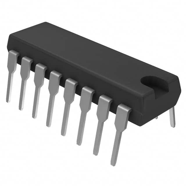
- Part No.:
- HCF4089BEY
- Manufacturer:
- STMicroelectronics
- Category:
- Specialty Logic
- Package:
- 16-DIP (0.300", 7.62mm)
- Datasheet:
-
 HCF4089BEY.pdf
- Description:
- IC MULTIPLIER BINARY 16-DIP
- Quantity:
- Payment:

- Shipping:

Inventory:3,539
Please send an inquiry. Send us your inquiry, and we will respond immediately.
Product details
Overview
HCF4089BEY from STMicroelectronics is a B-series CMOS 4-bit binary rate multiplier IC that generates an output pulse train equal to (N/16) × clock input rate, where N is the 4-bit binary input (0–15). It features cascading capability, synchronous internal counter, SET-to-15 and "15" detect outputs, and operates from 3V to 20V supply. Used in analog function generation, A/D-D/A conversion, and frequency division circuits.
For engineers reviewing the HCF4089BEY datasheet, HCF4089BEY pinout, HCF4089BEY application, or HCF4089BEY equivalent, key selection criteria include its 4-bit rate multiplication ratio, cascading support for multi-digit operations, quiescent current ≤600 µA at 20V, and DIP-16 package compatibility with legacy industrial timing and control designs.
Technical Context
The HCF4089BEY implements a synchronous 4-bit counter combined with combinational logic to produce deterministic pulse trains based on the A/B/C/D inputs. Its output duty cycle is precisely controlled by the binary weight of each input bit, enabling linear interpolation between integer multiples of 1/16 clock rate.
It supports two cascading modes-ADD and MULTIPLY-via CASCADE, INHIBIT IN/OUT, and STROBE signals, allowing expansion to 8-bit or higher resolution rate multiplication without external logic. The SET and CLEAR inputs provide synchronous initialization and reset under system control.
Key Specifications
| Parameter | Value and Actual Design Meaning |
|---|---|
| Rate Multiplication Ratio | N/16 (N = 0–15), enabling precise fractional clock division or analog waveform synthesis |
| Supply Voltage Range | 3 V to 20 V - supports wide-voltage industrial and legacy 5/10/15 V systems |
| Quiescent Current | ≤600 µA at VDD = 20 V - ensures low-power operation in battery-backed or energy-constrained designs |
| Max Clock Frequency | 7 MHz at VDD = 15 V - sets upper limit for real-time rate modulation bandwidth |
| Propagation Delay (CLOCK→OUT) | 90 ns (typ.) at VDD = 15 V - defines timing resolution for synchronized pulse generation |
| Input Leakage Current | ±0.1 µA max at VDD = 18 V - guarantees reliable logic-level integrity in high-impedance control paths |
| Noise Margin | 2.5 V min at VDD = 15 V - ensures robust noise immunity in electrically noisy environments |
Pinout & Package
Package: Plastic DIP-16 (0.300 inch width), 20 mm × 8.5 mm body, 2.54 mm lead pitch, through-hole mounting.
| Pin/Terminal | Circuit Role | Design Meaning |
|---|---|---|
| 1 | "15" OUT | Active-high flag indicating when all four rate-select bits (A–D) are high (N = 15) |
| 2–3, 14–15 | A, B, C, D | 4-bit parallel binary rate select inputs (LSB = A, MSB = D) |
| 4 | SET TO "15" | Synchronous load input forcing internal counter to state 15 on next CLOCK edge |
| 5–6 | OUT | Dual open-drain or totem-pole rate output pins (identical function, may be paralleled) |
| 7 | INHIBIT OUT (CARRY) | Carry-out signal active when internal counter overflows after 16 clocks |
| 9 | CLOCK | Positive-edge-triggered master timing input controlling pulse generation timing |
| 10 | STROBE | Edge-triggered latch enabling synchronous capture of A–D inputs into internal register |
| 11 | INHIBIT IN (CARRY) | Cascade carry-in for multi-stage ADD/MULTIPLY mode synchronization |
| 12 | CASCADE | Mode-select input determining whether device operates in ADD or MULTIPLY cascade configuration |
| 13 | CLEAR | Asynchronous reset clearing internal counter and outputs to zero state |
| 8 | VSS | Negative supply reference (ground) for all logic and output stages |
| 16 | VDD | Positive supply rail (3–20 V) powering CMOS logic and output drivers |
Key Features
| Feature | Design Value |
|---|---|
| Cascadable 4-bit architecture | Enables scalable rate multiplication up to 8+ bits using ADD or MULTIPLY interconnection modes |
| Synchronous SET and CLEAR | Ensures deterministic initialization and restart without race conditions or metastability |
| Dual OUT pins with symmetrical drive | Allows current sharing or redundant routing to improve signal integrity in noisy layouts |
| 100% tested quiescent current | Guarantees low-power performance across full voltage range (3–20 V) without binning |
| JEDEC JESD13B compliant | Meets standardized B-series CMOS electrical and mechanical specifications for interoperability |
Applications
| Function Generator | Analog-Digital Converter Interface |
|---|---|
Use Scenario: Generating variable-duty-cycle waveforms for calibration, testing, or actuator control in lab equipment. IC Role / Device Role / Timing Role: Rate multiplier acting as programmable pulse-density modulator with 1/16-step resolution. Use Value: Enables accurate emulation of analog voltages via digital control without DAC hardware, reducing BOM cost and board space. | Use Scenario: Interfacing microcontroller GPIOs to legacy analog subsystems requiring time-based voltage representation. IC Role / Device Role / Timing Role: Digital-to-time converter translating 4-bit digital codes into proportional pulse-width or pulse-frequency outputs. Use Value: Provides monotonic, linear transfer function (N/16) with no trimming required, simplifying firmware and eliminating calibration steps. |
| Frequency Division System | Multiplexed Signal Synthesis |
Use Scenario: Deriving sub-harmonic clock signals for mixed-signal ASIC test fixtures operating at non-integer clock ratios. IC Role / Device Role / Timing Role: Programmable divider generating exact fractions (e.g., 7/16, 13/16) of input clock frequency. Use Value: Delivers jitter-free, deterministic division ratios unattainable with standard counters or PLLs, improving test repeatability. | Use Scenario: Combining multiple HCF4089BEY units to synthesize complex periodic waveforms (e.g., logarithmic sweeps, sine approximations). IC Role / Device Role / Timing Role: Cascaded rate multiplier node in multi-stage ADD-mode configuration producing weighted superposition of pulse trains. Use Value: Achieves >16-step resolution (e.g., 256-step via dual-cascade) using only discrete logic, avoiding FPGA or microcontroller overhead. |
Equivalent & Alternatives
The following parts are listed as comparable options for similar binary rate multiplication applications.
| Alternative Part | Technical Difference | Application Difference | Selection Advice |
|---|---|---|---|
| CD4089BE | Pin-compatible but not JEDEC JESD13B certified; wider propagation delay variation (±50% vs ±30%) | Limited to commercial temperature range (0–70°C) vs industrial (-55–125°C) | Acceptable for cost-sensitive, non-critical consumer designs with stable ambient conditions |
| MC14089BDR2G | SOIC-16 only; lower max clock frequency (5 MHz @ 15 V); different inhibit/cascade logic polarity | Requires PCB redesign; incompatible with DIP-16 sockets and legacy through-hole assemblies | Preferred only when surface-mount assembly and tighter thermal management are mandatory |
Compared with CD4089BE and MC14089BDR2G, the HCF4089BEY offers guaranteed industrial temperature operation, JEDEC-compliant parametric stability, and direct DIP-16 drop-in replacement capability-making it the sole choice for field-deployed, long-lifecycle instrumentation and control systems.
Availability
HCF4089BEY is available at Aetrix Electronics and suitable for precision waveform generation, legacy industrial controller upgrades, and analog interface retrofitting requiring stable component supply and long-term obsolescence mitigation.
Supply support for HCF4089BEY includes scheduled delivery planning, volume procurement assistance, BOM continuity management, traceable sourcing, and lifecycle availability coordination for OEM customers, industrial embedded developers, connected-device designers, and electronics production programs.
Manufacturer
STMicroelectronics is a global semiconductor leader headquartered in Geneva, Switzerland, specializing in automotive, industrial, and power management ICs with strong heritage in CMOS logic and analog-mixed-signal design.
The HCF4089BEY belongs to ST's legacy HCF4000B series of radiation-hardened, high-voltage-tolerant CMOS logic devices engineered for reliability in harsh industrial, aerospace, and test equipment environments.
FAQ
What is the function of the CASCADE pin on HCF4089BEY?
The CASCADE pin selects between ADD and MULTIPLY cascading modes when connecting multiple HCF4089BEY devices. In ADD mode, it enables summing of fractional rates (e.g., 11/16 + 13/256); in MULTIPLY mode, it configures the device for two-variable multiplication (A × B)/256. Its logic level determines internal carry path routing and must be set before enabling STROBE.
Can HCF4089BEY operate at 3.3 V?
No-HCF4089BEY is specified for minimum VDD = 3 V, but its DC and dynamic parameters (e.g., VOH, fCL, tPD) are only guaranteed from VDD = 5 V onward per the datasheet. At 3.3 V, output drive strength, noise margin, and maximum clock frequency degrade significantly and are not characterized; use only within the validated 5–20 V range.
How does the SET TO "15" input differ from the CLEAR input?
SET TO "15" is a synchronous load command that forces the internal 4-bit counter to state 15 on the next rising CLOCK edge, preserving timing alignment. CLEAR is asynchronous and immediately resets the counter and outputs to zero regardless of clock phase-introducing potential glitches if asserted mid-cycle. SET enables predictable initialization; CLEAR provides emergency reset.
Why are there two OUT pins (pins 5 and 6)?
Pins 5 and 6 are electrically identical rate output terminals provided for layout flexibility and current handling. They may be wired in parallel to double sink/source capability (up to ±6.8 mA at VDD = 15 V), or used separately for differential signaling or redundancy. No internal logic distinction exists-the same pulse train appears on both pins simultaneously.
HCF4089BEY Specifications
- Product attributes
- Attribute value
- Manufacturer:
- STMicroelectronics
- Series:
- 4000B
- Package/Case:
- 16-DIP (0.300", 7.62mm)
- Packaging:
- Tube
- Product Status:
- Obsolete
- Logic Type:
- Binary Rate Multiplier
- Supply Voltage:
- 3V ~ 20V
- Number of Bits:
- 4
- Operating Temperature:
- -55°C ~ 125°C
- Grade:
- -
- Qualification:
- -
- Mounting Type:
- Through Hole
- Supplier Device Package:
- 16-DIP
HCF4089BEY FAQ
1.How can I place an order for HCF4089BEY through Aetrix?
Please submit a Request for Quotation (RFQ) for HCF4089BEY on Aetrix. Our sales agent will provide a competitive quotation and guide you through the order confirmation once you accept the terms.
2.Are the price and stock information for HCF4089BEY reliable?
The price and inventory of HCF4089BEY are updated periodically and may fluctuate due to market conditions. Stock and pricing data are typically refreshed every 24 hours. Quotation validity for HCF4089BEY is usually 5 days.
3.What payment methods are accepted for HCF4089BEY?
We accept Wire Transfer, PayPal, Credit Card, Western Union, MoneyGram, and Escrow for HCF4089BEY transactions.
Note: Certain payment methods may incur a processing fee.
4.How is shipping managed for HCF4089BEY?
HCF4089BEY orders can be shipped via leading logistics carriers, including DHL, UPS, FedEx, TNT, or Registered Mail.
Once your HCF4089BEY order is processed, you will receive an email with the shipment details and tracking number.
Note: Tracking information may take up to 24 hours to appear. Express delivery typically takes 3–5 business days.
5.How can I obtain technical support or documentation for HCF4089BEY?
For technical support, including HCF4089BEY datasheets, pinout diagrams, or application guidance, please contact our engineering support team. They can provide detailed documentation and assistance for your HCF4089BEY requirements.
6.How does Aetrix verify that HCF4089BEY is sourced from the original manufacturer or authorized distributors?
All HCF4089BEY products on Aetrix are procured from qualified distributors and authorized channels. Our dedicated quality assurance team conducts strict verification, including traceability checks and, if necessary, third-party testing. This ensures that HCF4089BEY meets industry standards.
7.What is the process for return or replacement of HCF4089BEY?
All HCF4089BEY units undergo pre-shipment inspection (PSI). If there is an issue with HCF4089BEY, returns or replacements are accepted under the following conditions:
1.Quantity discrepancies, incorrect items, or visible external defects (such as breakage or corrosion), acknowledged by Aetrix.
2.The issue is reported within 90 days of delivery.
3.The HCF4089BEY part is unused and in its original packaging.
Return procedure for HCF4089BEY:
1.Submit a request within 90 days.
2.Obtain a Return Material Authorization (RMA) from Aetrix.
HCF4089BEY Tags

-
MC14490DWR2G
onsemi
-
SY58600UMG-TR
Microchip Technology

-
MC100EP16DTR2G
onsemi
-
MC100EP16MNR4G
onsemi
-
74LVC1GX04GW,125
Nexperia USA Inc.

-
CD4007UBE
Texas Instruments
-
NXS0104PWJ
Nexperia USA Inc.

-
CD74HC283M96
Texas Instruments

-
SN74LVC1GX04DCKR
Texas Instruments

-
SN74F283N
Texas Instruments
-
SN74LVC1404DCTR
Texas Instruments

-
SN74LVC1GX04DBVR
Texas Instruments
Tech Hub

A practical engineering and sourcing framework covering lifecycle verification, lifetime-buy calculations, replacement qualification, supplier checks and counterfeit-risk controls.

TTL and CMOS logic families differ in thresholds, loading, output drive, power and timing. This engineering guide compares 74HC and 74HCT, calculates noise margins and checks 3.3 V/5 V compatibility.

A practical engineering guide to 3.3V and 5V logic compatibility, input thresholds, resistor dividers, translator ICs, MOSFET level shifting, I2C pull-ups, timing limits and power-sequencing risks.

The 74HC595 uses push-pull logic outputs, while the TPIC6B595 uses 50 V open-drain DMOS sinks for higher-power loads. This guide compares timing, current limits, 3.3 V interfacing, load wiring, thermal…

The 74HC595 converts serial data into eight stable parallel outputs. This guide covers pin functions, shift and storage timing, OE and MR behavior, drive-current limits, cascading, voltage compatibilit…

A technical comparison of level-sensitive latches and edge-triggered flip-flops, covering timing windows, setup and hold limits, master–slave operation, time borrowing, race-through, HDL inference and…

A D latch stores one bit while Enable controls when data can pass. This reference covers gate-level operation, truth tables, transparency, setup and hold timing, LE versus OE, common ICs and practical …

An SR latch stores one bit through cross-coupled feedback. This engineering reference covers NOR and NAND implementations, truth tables, forbidden-state recovery, gated operation, switch debouncing, fa…

Latch circuits retain one bit through feedback. This technical reference covers SR and D latches, truth tables, transparency, timing limits, latch-versus-flip-flop behavior, applications and common log…

An engineering guide to LED driver operation, constant-current and constant-voltage outputs, linear and switching topologies, dimming, IC selection, calculations, replacement compatibility, and fault c…


