
 My Inquiry
 My Account


onsemi HCPL2630SV
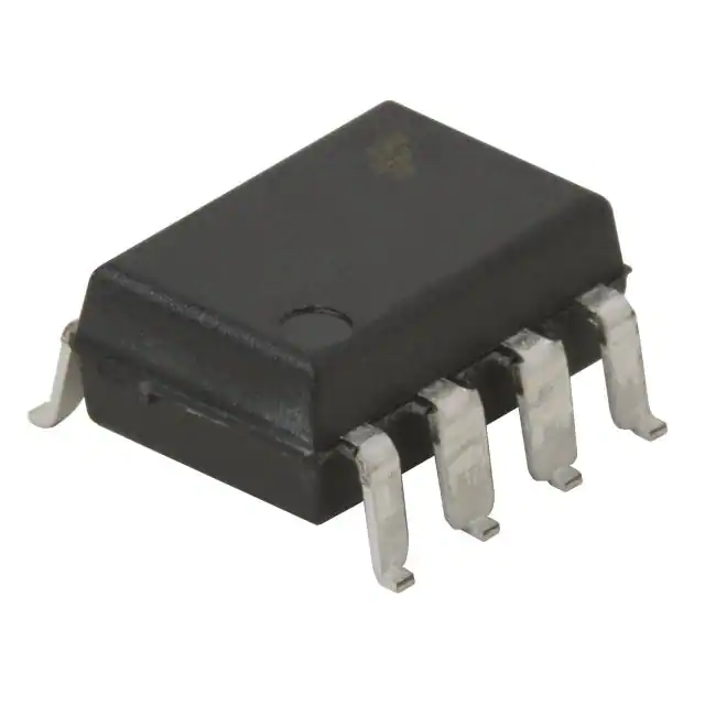
- Part No.:
- HCPL2630SV
- Manufacturer:
- onsemi
- Category:
- Logic Output Optoisolators
- Package:
- 8-SMD, Gull Wing
- Datasheet:
-
 HCPL2630SV.pdf
- Description:
- OPTOISO 2.5KV 2CH OPEN COLL 8SMD
- Quantity:
- Payment:

- Shipping:

Inventory:2,240
Please send an inquiry. Send us your inquiry, and we will respond immediately.
Product details
Overview
HCPL2630SV from ON Semiconductor (formerly Fairchild) is a dual-channel, high-speed logic gate optocoupler with 10 Mbit/s data rate, 10 kV/µs common-mode transient immunity, and open-collector strobable outputs. It isolates digital signals between noisy power domains in industrial motor drives and isolated DC-DC feedback loops.
For engineers reviewing the HCPL2630SV datasheet, pinout, applications, or equivalent options, key selection criteria include dual-channel isolation integrity, propagation delay matching (<35 ns skew), enable-controlled output gating, and VDE 0884-certified reinforced insulation for IEC 61800-5-1 compliance.
Technical Context
The HCPL2630SV integrates two independent AlGaAs LED–photodetector–logic-gate channels in a single 8-pin DIP package. Each channel features a strobable open-collector output with internal pull-up, enabling wired-OR bus configurations and synchronized signal gating.
Its detector stage delivers TTL-compatible logic levels with fan-out of 8 over –40°C to +85°C, while the internal noise shield ensures 10 kV/µs CMR at both HIGH and LOW output states-guaranteed per channel under full temperature range.
Key Specifications
| Parameter | Value and Actual Design Meaning |
|---|---|
| Data Rate | 10 Mbit/s - supports RS-422/485 line receiver and isolated SPI clock transmission |
| Propagation Delay | TPLH/TPHL = 20–75 ns - enables sub-100 ns timing-critical gate drive isolation |
| CMR | 10 kV/µs - maintains signal integrity in high-dV/dt environments like IGBT gate drivers |
| Fan-out | 8 TTL loads - drives multiple downstream logic stages without external buffers |
| Isolation Voltage | 2500 VRMS - meets reinforced insulation requirements for functional safety up to 480 V working voltage |
| Enable Control | Strobable input per channel - allows synchronous blanking during power stage switching transitions |
| VDE Certification | VDE 0884-10 - certified for reinforced insulation, supporting IEC 61800-5-1 and IEC 62368-1 system-level compliance |
Pinout & Package
HCPL2630SV uses an 8-pin plastic DIP package (0.300" wide) with gull-wing surface-mount leads (SMD variant). Pin 1 is marked with dot; pins 1–4 form Input Side A/B; pins 5–8 form Output Side common to both channels.
| Pin/Terminal | Circuit Role | Design Meaning |
|---|---|---|
| 1, 4 | Input Anode A / B | LED anodes - require current-limiting resistor; dual independent inputs |
| 2, 3 | Input Cathode A / B | LED cathodes - connect to ground or low-side switch for channel activation |
| 5 | GND | Output-side ground reference - must be decoupled with 0.1 µF capacitor to pin 8 |
| 6, 7 | VO1 / VO2 | Open-collector outputs - sink up to 13 mA each; require external pull-up for logic HIGH |
| 8 | VCC | Output-side supply - 4.5–5.5 V; bypassed to GND (pin 5) for noise suppression |
Key Features
| Feature | Design Value |
|---|---|
| Dual independent channels | Enables isolated control of two power switches (e.g., half-bridge high/low side) in one package |
| Strobable enable per channel | Allows precise timing control of output assertion-critical for dead-time management in inverters |
| Wired-OR open-collector outputs | Supports bus arbitration and fault signaling across multiple isolated subsystems |
| VDE 0884-10 certification | Validated reinforced insulation eliminates need for external creepage/clearance design effort |
| 10 kV/µs CMR (min) | Prevents false triggering in high-noise motor drive and SMPS applications with fast-switching GaN/SiC devices |
Applications
| Industrial Motor Drive | Isolated DC-DC Feedback |
|---|---|
|
Use Scenario: Gate driving IGBTs in three-phase VFDs with isolated PWM inputs and fault feedback. IC Role / Device Role / Timing Role: Dual-channel isolator providing independent, time-synchronized gate signals and desaturation fault reporting. Use Value: Enables compact half-bridge driver layout with matched propagation delays (<35 ns inter-channel skew) and VDE-certified safety isolation. |
Use Scenario: Transferring error amplifier output across primary-secondary boundary in flyback or forward converters. IC Role / Device Role / Timing Role: High-speed optocoupler replacing slower linear optos to improve loop bandwidth and transient response. Use Value: 10 Mbit/s data rate supports >1 MHz compensation loop closure; 10 kV/µs CMR rejects transformer leakage spikes. |
| Programmable Logic Controller I/O | Isolated Serial Interface |
|
Use Scenario: Isolating 24 V digital inputs from PLC CPU backplane in factory automation systems. IC Role / Device Role / Timing Role: Dual-channel logic gate optocoupler conditioning field sensor signals before FPGA/CPU sampling. Use Value: Fan-out of 8 drives multiple internal logic paths; strobable enable synchronizes sampling to scan cycle. |
Use Scenario: Level-shifting and isolating UART or SPI lines between MCU and isolated sensor nodes. IC Role / Device Role / Timing Role: Dual-channel isolator handling TX/RX paths or MOSI/MISO with independent enable control. Use Value: Wired-OR outputs allow multi-drop bus configuration; 20 ns min TPLH supports >5 Mbps serial rates. |
Equivalent & Alternatives
The following parts are listed as comparable options for similar dual-channel logic gate optocoupler applications.
| Alternative Part | Technical Difference | Application Difference | Selection Advice |
|---|---|---|---|
| ACPL-M61T | Single-channel, 10 MBd, 3750 VRMS isolation, no enable pin | Lacks dual-channel integration and strobable control; requires two units for same function | Use when only one isolated signal path needed and VDE certification not required |
| SI8660BD-B-IS | Dual-channel digital isolator, 100 MBd, 5000 VRMS, CMOS output, no optical coupling | No LED aging or CTR degradation; higher speed but lacks inherent galvanic noise rejection of photodiode stage | Prefer for long-life, high-reliability systems where optical lifetime is a concern and board space allows |
Compared with HCPL2630SV, ACPL-M61T requires duplication for dual-channel use and omits enable control, while SI8660BD-B-IS offers superior speed and lifetime but trades off the inherent common-mode noise resilience of optical coupling-making HCPL2630SV preferable in high-dV/dt industrial environments.
Availability
HCPL2630SV is available at Aetrix Electronics and suitable for industrial motor drives, isolated DC-DC feedback loops, and programmable logic controller I/O requiring stable component supply with VDE-certified reinforced insulation.
Supply support for HCPL2630SV includes scheduled delivery planning, volume procurement assistance, BOM continuity management, traceable sourcing, and lifecycle availability coordination for OEM customers, industrial embedded developers, connected-device designers, and electronics production programs.
Manufacturer
ON Semiconductor (formerly Fairchild Semiconductor) is a global semiconductor supplier focused on energy-efficient power, analog, sensing, and connectivity solutions for automotive, industrial, cloud, and consumer markets.
The HCPL2630SV belongs to the legacy Fairchild high-speed optocoupler family, designed specifically for robust digital signal isolation in harsh industrial environments with stringent safety and noise immunity requirements.
FAQ
What is the maximum operating temperature range for HCPL2630SV?
The HCPL2630SV is rated for continuous operation from –40°C to +85°C. All key parameters-including propagation delay, CMR, and fan-out-are guaranteed across this full industrial temperature range. Derating is not required within these limits, and thermal performance remains stable up to the upper bound.
Does HCPL2630SV require external pull-up resistors on its outputs?
Yes, HCPL2630SV has open-collector outputs (pins 6 and 7), so external pull-up resistors to VCC (pin 8) are mandatory to establish logic HIGH levels. Typical values range from 350 Ω to 4 kΩ depending on speed and load requirements; 350 Ω enables full 10 Mbit/s operation with 15 pF load.
Is HCPL2630SV pin-compatible with HCPL2631?
No, HCPL2630SV and HCPL2631 are not pin-compatible. HCPL2630SV has independent enable inputs per channel (pins 1 and 4 used as enables), while HCPL2631 uses shared enable (pin 3). Their pin functions differ fundamentally, and PCB layout cannot be reused between them without redesign.
What does the "SV" suffix indicate in HCPL2630SV?
The "SV" suffix denotes VDE 0884-10 certification and surface-mount packaging. "S" indicates gull-wing SMD leads, and "V" confirms VDE 0884-10 reinforced insulation approval-verified by test voltage of 2500 VRMS and partial discharge <5 pC at 1.2 × rated voltage.
Can HCPL2630SV replace 6N137 in a design?
No-HCPL2630SV is a dual-channel device with different pinout, enable architecture, and dual-output topology, whereas 6N137 is single-channel. Direct replacement would require circuit redesign. For dual-channel functionality, HCPL2630SV is purpose-built; for single-channel needs, 6N137SV is the direct VDE-certified counterpart.
HCPL2630SV Specifications
- Product attributes
- Attribute value
- Manufacturer:
- onsemi
- Series:
- -
- Package/Case:
- 8-SMD, Gull Wing
- Packaging:
- Tube
- Product Status:
- Obsolete
- Number of Channels:
- 2
- Inputs - Side 1/Side 2:
- 2/0
- Voltage - Isolation:
- 2500Vrms
- Common Mode Transient Immunity (Min):
- 10kV/µs (Typ)
- Input Type:
- DC
- Output Type:
- Open Collector
- Current - Output / Channel:
- 50 mA
- Data Rate:
- 10Mbps
- Propagation Delay tpLH / tpHL (Max):
- 75ns, 75ns
- Rise / Fall Time (Typ):
- 50ns, 12ns
- Voltage - Forward (Vf) (Typ):
- 1.4V
- Current - DC Forward (If) (Max):
- 30mA
- Voltage - Supply:
- 4.5V ~ 5.5V
- Grade:
- -
- Qualification:
- -
- Operating Temperature:
- -40°C ~ 85°C
- Mounting Type:
- Surface Mount
- Supplier Device Package:
- 8-SMD
HCPL2630SV FAQ
1.How can I place an order for HCPL2630SV through Aetrix?
Please submit a Request for Quotation (RFQ) for HCPL2630SV on Aetrix. Our sales agent will provide a competitive quotation and guide you through the order confirmation once you accept the terms.
2.Are the price and stock information for HCPL2630SV reliable?
The price and inventory of HCPL2630SV are updated periodically and may fluctuate due to market conditions. Stock and pricing data are typically refreshed every 24 hours. Quotation validity for HCPL2630SV is usually 5 days.
3.What payment methods are accepted for HCPL2630SV?
We accept Wire Transfer, PayPal, Credit Card, Western Union, MoneyGram, and Escrow for HCPL2630SV transactions.
Note: Certain payment methods may incur a processing fee.
4.How is shipping managed for HCPL2630SV?
HCPL2630SV orders can be shipped via leading logistics carriers, including DHL, UPS, FedEx, TNT, or Registered Mail.
Once your HCPL2630SV order is processed, you will receive an email with the shipment details and tracking number.
Note: Tracking information may take up to 24 hours to appear. Express delivery typically takes 3–5 business days.
5.How can I obtain technical support or documentation for HCPL2630SV?
For technical support, including HCPL2630SV datasheets, pinout diagrams, or application guidance, please contact our engineering support team. They can provide detailed documentation and assistance for your HCPL2630SV requirements.
6.How does Aetrix verify that HCPL2630SV is sourced from the original manufacturer or authorized distributors?
All HCPL2630SV products on Aetrix are procured from qualified distributors and authorized channels. Our dedicated quality assurance team conducts strict verification, including traceability checks and, if necessary, third-party testing. This ensures that HCPL2630SV meets industry standards.
7.What is the process for return or replacement of HCPL2630SV?
All HCPL2630SV units undergo pre-shipment inspection (PSI). If there is an issue with HCPL2630SV, returns or replacements are accepted under the following conditions:
1.Quantity discrepancies, incorrect items, or visible external defects (such as breakage or corrosion), acknowledged by Aetrix.
2.The issue is reported within 90 days of delivery.
3.The HCPL2630SV part is unused and in its original packaging.
Return procedure for HCPL2630SV:
1.Submit a request within 90 days.
2.Obtain a Return Material Authorization (RMA) from Aetrix.
HCPL2630SV Tags

-
6N137
Lite-On Inc.
-
6N137S
Lite-On Inc.
-
6N137S-TA1
Lite-On Inc.
.JPG)
-
TLP2362(TPR,E
Toshiba Semiconductor and Storage

-
H11L1M
onsemi
-
TLP2355(TPL,E
Toshiba Semiconductor and Storage
-
TLP2361(TPL,E
Toshiba Semiconductor and Storage
-
TLP2358(TPL,E)
Toshiba Semiconductor and Storage
-
H11L1SR2M
onsemi
-
TLP2361(V4-TPL,E
Toshiba Semiconductor and Storage
.JPG)
-
H11L1S(TA)
Everlight Electronics Co Ltd
-
H11L1SM
onsemi
Tech Hub

Counterfeit components can hide behind convincing markings and passing basic function tests. This engineering reference covers source traceability, external inspection, X-ray, XRF, electrical testing, …

A practical engineering and sourcing framework covering lifecycle verification, lifetime-buy calculations, replacement qualification, supplier checks and counterfeit-risk controls.

TTL and CMOS logic families differ in thresholds, loading, output drive, power and timing. This engineering guide compares 74HC and 74HCT, calculates noise margins and checks 3.3 V/5 V compatibility.

A practical engineering guide to 3.3V and 5V logic compatibility, input thresholds, resistor dividers, translator ICs, MOSFET level shifting, I2C pull-ups, timing limits and power-sequencing risks.

The 74HC595 uses push-pull logic outputs, while the TPIC6B595 uses 50 V open-drain DMOS sinks for higher-power loads. This guide compares timing, current limits, 3.3 V interfacing, load wiring, thermal…

The 74HC595 converts serial data into eight stable parallel outputs. This guide covers pin functions, shift and storage timing, OE and MR behavior, drive-current limits, cascading, voltage compatibilit…

A technical comparison of level-sensitive latches and edge-triggered flip-flops, covering timing windows, setup and hold limits, master–slave operation, time borrowing, race-through, HDL inference and…

A D latch stores one bit while Enable controls when data can pass. This reference covers gate-level operation, truth tables, transparency, setup and hold timing, LE versus OE, common ICs and practical …

An SR latch stores one bit through cross-coupled feedback. This engineering reference covers NOR and NAND implementations, truth tables, forbidden-state recovery, gated operation, switch debouncing, fa…

Latch circuits retain one bit through feedback. This technical reference covers SR and D latches, truth tables, transparency, timing limits, latch-versus-flip-flop behavior, applications and common log…


