
 My Inquiry
 My Account


Renesas HD6417750F167D
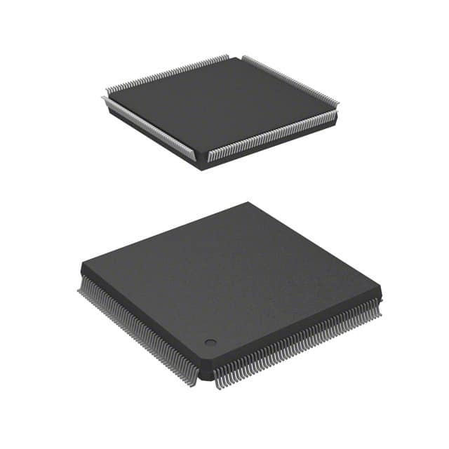
- Part No.:
- HD6417750F167D
- Manufacturer:
- Renesas
- Category:
- Microprocessors
- Package:
- -
- Datasheet:
-
 HD6417750F167D.pdf
- Description:
- RISC MPU, 32-BIT, 167MHZ
- Quantity:
- Payment:

- Shipping:

Inventory:434
Please send an inquiry. Send us your inquiry, and we will respond immediately.
Product details
Overview
HD6417750F167D from Renesas Electronics is a 32-bit RISC microprocessor in the SH7750S Group, implementing the SH-4 CPU core with integrated MMU, 16 KB instruction cache, 16 KB operand cache, and peripheral functions including dual serial interfaces (SCI/SCIF), RTC, UBC, BSC, and smart card interface. It operates at 167 MHz with 1.8 V core voltage and targets multimedia system-on-chip applications requiring real-time processing and memory management.
For engineers reviewing the HD6417750F167D datasheet, HD6417750F167D pinout, HD6417750F167D application, or HD6417750F167D equivalent, key selection criteria include its 208-pin QFP package, 167 MHz clock frequency, 1.8 V core supply, -20°C to +75°C operating temperature range, and compatibility with DRAM, SDRAM, and PCMCIA bus protocols.
Technical Context
The HD6417750F167D implements the SH-4 superscalar RISC architecture with five-stage pipeline, dual-issue capability, and IEEE 754-compliant floating-point unit. It integrates a 32-bit external data bus, 32-bit address bus, and supports big-endian memory organization.
Its memory management unit provides full virtual memory support with unified TLB, 64-entry ITLB, and 256-entry UTLB. The bus state controller enables direct interfacing with ROM, SRAM, DRAM, synchronous DRAM (including 64-bit 4-bank SDRAM), and PCMCIA devices without external glue logic.
Key Specifications
| Parameter | Value and Actual Design Meaning |
|---|---|
| Core Architecture | SH-4 32-bit RISC superscalar CPU with five-stage pipeline and dual-issue execution |
| Operating Frequency | 167 MHz - determines maximum instruction throughput and real-time response latency |
| Core Supply Voltage | 1.8 V - defines power delivery requirements and thermal design margin for sustained operation |
| Cache Memory | 16 KB instruction cache + 16 KB operand cache - reduces average memory access time and improves code/data fetch efficiency |
| Memory Management | MMU with 64-entry ITLB and 256-entry UTLB - enables full virtual memory support for OS-based embedded systems |
| Peripheral Integration | Dual serial interfaces (SCI/SCIF), RTC, user break controller (UBC), bus state controller (BSC), smart card interface - eliminates need for discrete support ICs in multimedia control designs |
| Bus Interface | 32-bit address / 32-bit data bus supporting ROM, SRAM, DRAM, SDRAM (64-bit 4-bank), PCMCIA - simplifies memory subsystem design with flexible timing configuration |
Pinout & Package
HD6417750F167D is housed in a 208-pin plastic quad flat pack (QFP) package with 0.5 mm lead pitch and standard JEDEC MO-140AC footprint. Thermal pad on underside requires proper PCB copper pour and via stitching for thermal management.
| Pin/Terminal | Circuit Role | Design Meaning |
|---|---|---|
| VDD, VSS | Power supply and ground | 1.8 V core supply pins (VDD) and dedicated ground returns (VSS); require local decoupling per Renesas layout guidelines |
| VDDQ, VSSQ | I/O power and ground | 3.3 V I/O supply (VDDQ) and associated ground (VSSQ); separate from core domain to support mixed-voltage signaling |
| CLK, EXTAL, XTAL | System clock input | Accepts external crystal (EXTAL/XTAL) or clock source (CLK); PLL generates internal 167 MHz core clock from base frequency |
| RESET, RES# | Reset control | Active-low asynchronous reset (RES#) and synchronous reset (RESET); both required for deterministic initialization sequence |
| A[31:0], D[31:0] | Address and data bus | 32-bit multiplexed address/data bus; requires external latch (e.g., 74LVC573) for demultiplexing in non-mux mode |
| RD#, WR#, CS#, OE#, WE# | Bus control signals | Standard read/write strobes and chip select enable precise timing control for memory and peripheral access |
| SCI0_TXD, SCI0_RXD, SCIF_TXD, SCIF_RXD | Serial communication | Dual independent UART-like interfaces: SCI0 supports basic async comms; SCIF adds FIFO and DMA-ready framing |
| RTC_CLK, RTC_ALM, RTC_SEC | Real-time clock | Dedicated 32.768 kHz oscillator input, alarm output, and second pulse output - enables battery-backed timekeeping without host intervention |
Key Features
| Feature | Design Value |
|---|---|
| Superscalar SH-4 Core | Enables dual-instruction issue per cycle, improving MIPS/Watt efficiency for multimedia codecs and real-time OS tasks |
| Integrated MMU with TLB | Supports full virtual memory mapping and context switching - essential for Linux, VxWorks, or other protected-mode RTOS deployments |
| On-chip Cache Hierarchy | Separate 16 KB instruction and 16 KB operand caches reduce external memory bandwidth demand by >60% in typical embedded workloads |
| Flexible Bus Controller (BSC) | Configurable wait-state generation and burst-length control allow seamless interfacing with diverse memory types without external logic |
| Dual Serial Interfaces | SCI0 for legacy device control and SCIF for high-throughput data streaming - enables concurrent debug, telemetry, and peripheral command channels |
| Smart Card Interface | Hardware-accelerated ISO/IEC 7816-3 protocol engine offloads bit-level timing and parity handling from CPU - critical for secure transaction systems |
Applications
| Digital Set-Top Box | Automotive Infotainment Head Unit |
|---|---|
|
Use Scenario: Real-time decoding of MPEG-2/4 video streams while managing conditional access, EPG, and UI rendering. IC Role / Device Role / Timing Role: Primary application processor executing OS kernel, media framework, and middleware with hardware-assisted cache and MMU. Use Value: 167 MHz SH-4 core delivers sufficient MIPS for SD video decode + UI compositing; integrated BSC eliminates bus arbitration logic for DDR SDRAM and NAND flash. |
Use Scenario: Central control unit coordinating audio playback, Bluetooth hands-free, navigation map rendering, and vehicle CAN bus diagnostics. IC Role / Device Role / Timing Role: System controller managing multi-threaded real-time tasks, peripheral I/O, and secure boot via smart card interface. Use Value: Dual serial interfaces enable simultaneous debug trace (SCI0) and Bluetooth HCI (SCIF); RTC and UBC support safe firmware update rollback and time-stamped logging. |
| Industrial HMI Terminal | Networked Media Player |
|
Use Scenario: Operator interface running Qt-based GUI with Modbus TCP gateway functionality over Ethernet PHY. IC Role / Device Role / Timing Role: Embedded application processor hosting Linux, driving LCD controller, and managing industrial protocol stacks. Use Value: MMU enables process isolation between GUI and protocol stack; 208-pin QFP allows cost-effective PCB routing with standard FR-4 stackup and no BGA rework complexity. |
Use Scenario: Streaming audio/video over UPnP/DLNA with local storage access, metadata parsing, and remote control via IR/RF. IC Role / Device Role / Timing Role: Media-centric SoC managing file I/O, codec acceleration, network stack, and real-time playback scheduling. Use Value: Integrated SCIF supports high-speed USB-to-serial bridge for mass storage class; BSC timing registers configure NAND flash with variable read latency for wear-leveling algorithms. |
Equivalent & Alternatives
The following parts are listed as comparable options for similar 32-bit RISC microprocessor applications.
| Alternative Part | Technical Difference | Application Difference | Selection Advice |
|---|---|---|---|
| HD6417750SF200 | 200 MHz operation, same 208-pin QFP package, 1.8 V core, identical peripheral set | Higher performance for compute-intensive video encoding or multi-zone audio processing | Select when application requires >167 MHz sustained throughput and thermal headroom permits higher power dissipation |
| HD6417750SVF133 | 133 MHz operation, 1.5 V core, same 208-pin QFP, identical feature set except lower frequency and voltage | Lower power consumption for fanless or thermally constrained portable media devices | Select when system-level power budget limits active power to ≤1.2 W and real-time deadlines permit relaxed timing margins |
Compared with HD6417750F167D, HD6417750SF200 offers 20% higher clock rate for latency-critical tasks but increases dynamic power by ~35%; HD6417750SVF133 reduces core voltage to 1.5 V, cutting static power by 31% at the cost of 20% lower throughput - enabling trade-offs between performance density and thermal envelope.
Availability
HD6417750F167D is available at Aetrix Electronics and suitable for digital set-top boxes, automotive infotainment systems, and industrial HMI terminals requiring stable component supply across extended production lifecycles.
Supply support for HD6417750F167D includes scheduled delivery planning, volume procurement assistance, BOM continuity management, traceable sourcing, and lifecycle availability coordination for OEM customers, industrial embedded developers, connected-device designers, and electronics production programs.
Manufacturer
Renesas Electronics Corporation is a global semiconductor manufacturer specializing in microcontrollers, analog, power, and SoC solutions for automotive, industrial, and consumer markets.
The SH7750 Series was designed as a high-performance 32-bit RISC microprocessor platform for multimedia-rich embedded systems, emphasizing integration of memory management, caching, and peripheral controllers to reduce system-level BOM and board area.
FAQ
What is the maximum operating temperature specification for HD6417750F167D?
The HD6417750F167D is rated for operation from –20°C to +75°C ambient temperature. This specification applies to the standard version documented in the R01UH0456EJ0702 Rev. 7.02 Hardware Manual. Extended temperature variants (–40°C to +85°C) are available under different part numbers such as HD6417750RBA240HV, but HD6417750F167D itself does not support the extended range.
Does HD6417750F167D support DDR SDRAM directly?
HD6417750F167D does not support DDR SDRAM natively. Its bus state controller (BSC) supports standard SDRAM (including 64-bit 4-bank configurations) and asynchronous memory types, but lacks the DLL, bidirectional DQS, and command encoding required for DDR. Designers must use external memory controller ASICs or FPGAs to interface DDR SDRAM with HD6417750F167D.
Is the smart card interface on HD6417750F167D compliant with ISO/IEC 7816-3?
Yes, the smart card interface on HD6417750F167D implements full hardware support for ISO/IEC 7816-3 asynchronous T=0 protocol, including automatic guard time insertion, character parity checking, and clock frequency adaptation. It does not support T=1 or contactless protocols - those require external co-processors or dedicated secure elements.
What debug capabilities does HD6417750F167D provide?
HD6417750F167D includes a User Break Controller (UBC) supporting hardware breakpoints, watchpoints, and trace trigger events. It works with Renesas E1/E20 emulators and compatible JTAG debuggers. The UBC supports up to four independent address-match conditions and integrates with the SH-4's on-chip debug architecture for non-intrusive real-time analysis without software instrumentation.
Can HD6417750F167D execute code directly from external NOR flash without copying to RAM?
Yes, HD6417750F167D supports XIP (eXecute-In-Place) from external NOR flash via its bus state controller. The BSC allows configurable wait states, burst length, and access timing to match flash characteristics. However, instruction cache coherency must be managed manually when flash contents change - the cache does not auto-invalidate on external writes.
HD6417750F167D Specifications
- Product attributes
- Attribute value
- Manufacturer:
- Renesas
- Package/Case:
- -
- Series:
- *
- Packaging:
- Bulk
- Product Status:
- Active
- Core Processor:
- -
- Number of Cores/Bus Width:
- -
- Speed:
- -
- Co-Processors/DSP:
- -
- RAM Controllers:
- -
- Graphics Acceleration:
- -
- Display & Interface Controllers:
- -
- Ethernet:
- -
- SATA:
- -
- USB:
- -
- Voltage - I/O:
- -
- Operating Temperature:
- -
- Grade:
- -
- Qualification:
- -
- Security Features:
- -
- Mounting Type:
- -
- Supplier Device Package:
- -
- Additional Interfaces:
- -
HD6417750F167D FAQ
1.How can I place an order for HD6417750F167D through Aetrix?
Please submit a Request for Quotation (RFQ) for HD6417750F167D on Aetrix. Our sales agent will provide a competitive quotation and guide you through the order confirmation once you accept the terms.
2.Are the price and stock information for HD6417750F167D reliable?
The price and inventory of HD6417750F167D are updated periodically and may fluctuate due to market conditions. Stock and pricing data are typically refreshed every 24 hours. Quotation validity for HD6417750F167D is usually 5 days.
3.What payment methods are accepted for HD6417750F167D?
We accept Wire Transfer, PayPal, Credit Card, Western Union, MoneyGram, and Escrow for HD6417750F167D transactions.
Note: Certain payment methods may incur a processing fee.
4.How is shipping managed for HD6417750F167D?
HD6417750F167D orders can be shipped via leading logistics carriers, including DHL, UPS, FedEx, TNT, or Registered Mail.
Once your HD6417750F167D order is processed, you will receive an email with the shipment details and tracking number.
Note: Tracking information may take up to 24 hours to appear. Express delivery typically takes 3–5 business days.
5.How can I obtain technical support or documentation for HD6417750F167D?
For technical support, including HD6417750F167D datasheets, pinout diagrams, or application guidance, please contact our engineering support team. They can provide detailed documentation and assistance for your HD6417750F167D requirements.
6.How does Aetrix verify that HD6417750F167D is sourced from the original manufacturer or authorized distributors?
All HD6417750F167D products on Aetrix are procured from qualified distributors and authorized channels. Our dedicated quality assurance team conducts strict verification, including traceability checks and, if necessary, third-party testing. This ensures that HD6417750F167D meets industry standards.
7.What is the process for return or replacement of HD6417750F167D?
All HD6417750F167D units undergo pre-shipment inspection (PSI). If there is an issue with HD6417750F167D, returns or replacements are accepted under the following conditions:
1.Quantity discrepancies, incorrect items, or visible external defects (such as breakage or corrosion), acknowledged by Aetrix.
2.The issue is reported within 90 days of delivery.
3.The HD6417750F167D part is unused and in its original packaging.
Return procedure for HD6417750F167D:
1.Submit a request within 90 days.
2.Obtain a Return Material Authorization (RMA) from Aetrix.
HD6417750F167D Tags

-
AT91SAM9260B-CU-999
Microchip Technology
-
AT91SAM9G25-CU
Microchip Technology

-
ATSAMA5D27C-CU
Microchip Technology
-
AT91SAM9X35-CU
Microchip Technology
-
AT91SAM9X25-CU
Microchip Technology

-
MCIMX6Y2CVM08AB
NXP Semiconductors
.JPG)
-
AM3352BZCZ100
Texas Instruments
-
AT91SAM9260B-CU
Microchip Technology

-
AT91SAM9260B-QU
Microchip Technology

-
ATSAMA5D31A-CU
Microchip Technology
-
AT91SAM9G20B-CU-999
Microchip Technology
-
MCIMX6Y2CVM05AB
NXP Semiconductors
Tech Hub

TTL and CMOS logic families differ in thresholds, loading, output drive, power and timing. This engineering guide compares 74HC and 74HCT, calculates noise margins and checks 3.3 V/5 V compatibility.

A practical engineering guide to 3.3V and 5V logic compatibility, input thresholds, resistor dividers, translator ICs, MOSFET level shifting, I2C pull-ups, timing limits and power-sequencing risks.

The 74HC595 uses push-pull logic outputs, while the TPIC6B595 uses 50 V open-drain DMOS sinks for higher-power loads. This guide compares timing, current limits, 3.3 V interfacing, load wiring, thermal…

The 74HC595 converts serial data into eight stable parallel outputs. This guide covers pin functions, shift and storage timing, OE and MR behavior, drive-current limits, cascading, voltage compatibilit…

A technical comparison of level-sensitive latches and edge-triggered flip-flops, covering timing windows, setup and hold limits, master–slave operation, time borrowing, race-through, HDL inference and…

A D latch stores one bit while Enable controls when data can pass. This reference covers gate-level operation, truth tables, transparency, setup and hold timing, LE versus OE, common ICs and practical …

An SR latch stores one bit through cross-coupled feedback. This engineering reference covers NOR and NAND implementations, truth tables, forbidden-state recovery, gated operation, switch debouncing, fa…

Latch circuits retain one bit through feedback. This technical reference covers SR and D latches, truth tables, transparency, timing limits, latch-versus-flip-flop behavior, applications and common log…

An engineering guide to LED driver operation, constant-current and constant-voltage outputs, linear and switching topologies, dimming, IC selection, calculations, replacement compatibility, and fault c…

Operational amplifier guide covering op amp basics, feedback, ideal vs real op amps, common configurations, buffer circuits, offset, bias current, gain-bandwidth, slew rate, rail-to-rail limits and sel…


