
 My Inquiry
 My Account


Renesas HD64413ASFV
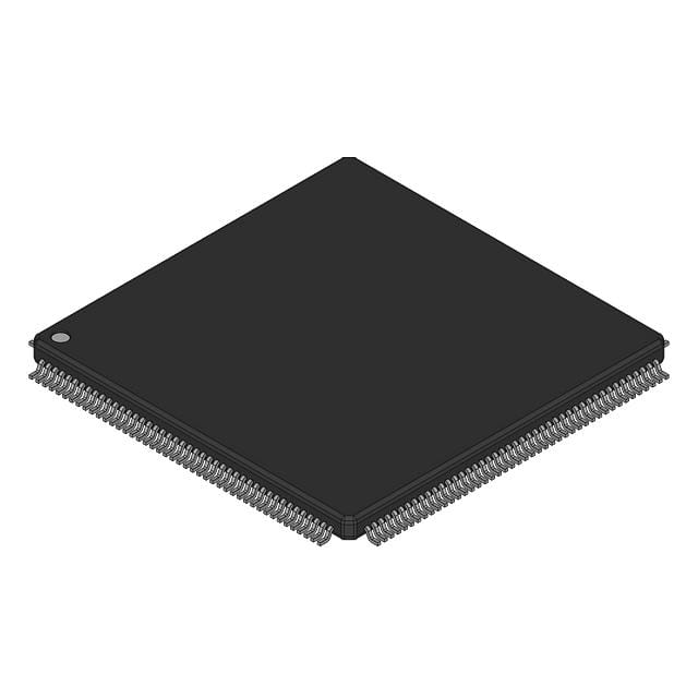
- Part No.:
- HD64413ASFV
- Manufacturer:
- Renesas
- Category:
- Microprocessors
- Package:
- -
- Datasheet:
-
 HD64413ASFV.pdf
- Description:
- GRAPHICS PROCESSOR
- Quantity:
- Payment:

- Shipping:

Inventory:597
Please send an inquiry. Send us your inquiry, and we will respond immediately.
Product details
Overview
HD64413ASFV from Renesas Technology Corp. is a SuperH RISC-based peripheral LSI functioning as a dedicated 2D graphics renderer with integrated synchronous DRAM interface, supporting real-time polygon rendering, video capture (YCbCr/RGB), display composition, and CRT/video encoder output. It operates at 50 MHz system clock, supports 16-bit CPU bus interface, and integrates Unified Graphics Memory (UGM) architecture for double-buffered screen updates in multimedia terminals.
For engineers reviewing the HD64413ASFV datasheet, HD64413ASFV pinout, HD64413ASFV application, or HD64413ASFV equivalent, key selection criteria include its Q2SD-series UGM memory mapping, SDRAM timing compatibility (CAS latency 2–3), video input interface support (ITU-R BT.656 compliant), and register-level command execution model for display list processing.
Technical Context
The HD64413ASFV implements a hardware-accelerated Unified Graphics Memory (UGM) architecture that decouples rendering commands from display refresh via dual-port memory access arbitration between CPU, DMAC, and internal Q2SD engine. It supports three concurrent memory domains: display buffer, work buffer, and video capture buffer - each independently addressable within a 32-bit UGM space.
Its rendering pipeline executes fixed-function 2D primitives (POLYGON4A/B/C, LINE, FTRAP) fetched from display lists stored in SDRAM, with real-time clipping, color expansion (256-color palette), and coordinate transformation. Video capture operates in parallel with rendering, supporting programmable window size (up to 720×480), YCbCr-to-RGB conversion, and subsampling control.
Key Specifications
| Parameter | Value and Actual Design Meaning |
|---|---|
| Core Architecture | SuperH RISC engine peripheral LSI - no embedded CPU core; requires external SH microcontroller for command issuance and register control. |
| Graphics Engine | Q2SD (Quick 2D Graphics Renderer) - executes display list commands in hardware without CPU intervention during rendering phase. |
| Memory Interface | Synchronous DRAM (SDRAM) interface - supports 16-bit data bus, 128-Mbit max capacity, CAS latency 2 or 3, burst length 1/2/4/8. |
| Video Input | ITU-R BT.656-compatible 8-/16-bit parallel interface - captures NTSC/PAL video with programmable start position and reduction scaling. |
| Display Output | Programmable CRT/video encoder interface - supports RGB analog output, composite video, and sync signals (HSYNC/VSYNC/BLANK). |
| Color Handling | 256-entry × 24-bit color palette (CP000R–CP255R registers) - enables palette-based display with per-pixel index lookup and color offset adjustment. |
| Interrupt Support | Dedicated interrupt outputs (INT0–INT2) - signals display vertical blank, command completion, video frame capture ready, and error conditions. |
Pinout & Package
HD64413ASFV is housed in a 208-pin PQFP (Plastic Quad Flat Package) with 0.5 mm pitch, thermally enhanced for graphics-intensive operation. Pin functions are grouped into system control, CPU interface (16-bit data, 24-bit address), UGM/SDRAM interface, display output (RGB, sync), video input (Y/Cb/Cr, CLK, VLD), and power/ground domains.
| Pin/Terminal | Circuit Role | Design Meaning |
|---|---|---|
| CLKIN | System Clock Input | Accepts 50 MHz single-ended clock; drives internal PLL for UGM timing and display sync generation. |
| RESET | Active-Low Reset | Asynchronous reset pin - initializes all registers, disables outputs, and clears UGM state until deasserted. |
| CS0#, CS1# | Chip Select Inputs | Decode HD64413ASFV address space on 16-bit CPU bus; CS0# selects register map, CS1# selects display list memory region. |
| RD#, WR#, RDY | CPU Bus Control | Standard asynchronous read/write handshake signals - RDY extends cycle when UGM arbitration delays access. |
| SDCKE, SDCK, SDCAS#, SDRAS#, SDWE# | SDRAM Command Interface | Direct control of SDRAM mode register, row/column activation, and write enable - no external SDRAM controller required. |
| R/G/B[7:0], HSYNC, VSYNC, BLANK | Display Output Drivers | 8-bit RGB analog-ready outputs with sync signals - require external DACs and termination for CRT or encoder interface. |
| Y[7:0], Cb[7:0], Cr[7:0], VLD, CLK27 | Video Capture Inputs | Parallel YCbCr 4:2:2 data stream with 27 MHz pixel clock and valid line signal - supports interlaced/progressive capture. |
Key Features
| Feature | Design Value |
|---|---|
| Unified Graphics Memory (UGM) | Single SDRAM space shared across display, work, and video buffers with hardware-enforced double-buffering and refresh control. |
| Display List Execution Engine | Hardware parser fetches and executes POLYGON4, LINE, CLRW, JUMP, and GOSUB commands from SDRAM without CPU overhead. |
| Real-Time Video Capture | On-the-fly YCbCr-to-RGB conversion, programmable capture window (16×16 to 720×480), and subsampling (½×, ¼×) for preview scaling. |
| Multi-Mode Display Composition | Overlays video, graphics, and cursor layers with independent clipping, transparency, and palette-based color blending. |
| Register-Level Interrupt Management | Configurable INT0–INT2 outputs tied to specific events (e.g., VBLANK, CMD_DONE, CAPTURE_READY) with maskable enable bits in IER. |
Applications
| Set-Top Box GUI Rendering | Industrial HMI Display Controller |
|---|---|
Use Scenario: Real-time rendering of interactive menus, channel banners, and EPG overlays atop live TV video feed. IC Role / Device Role / Timing Role: Dedicated graphics accelerator handling polygon fill, alpha-blended text, and video compositing while external SH CPU manages navigation logic. Use Value: Eliminates CPU load for 2D rendering tasks, enabling sub-16ms frame update with synchronized video capture and display output. | Use Scenario: Operator interface for factory automation panels requiring high-reliability graphical status indicators and alarm overlays. IC Role / Device Role / Timing Role: Standalone display controller managing CRT output, touch-screen coordinate mapping, and non-volatile palette storage. Use Value: Provides deterministic display timing and hardware double-buffering to prevent screen tearing during dynamic UI updates. |
| Medical Imaging Preview Terminal | Digital Signage Content Player |
Use Scenario: Low-latency preview of ultrasound or endoscopy video streams with annotation overlays (scale bars, ROI markers). IC Role / Device Role / Timing Role: Video capture + graphics co-processor generating calibrated RGB output for medical-grade monitors. Use Value: Supports ITU-R BT.656 video input and precise pixel-aligned overlay rendering without frame buffering delay. | Use Scenario: Embedded signage player rendering animated advertisements with layered bitmap content and video backgrounds. IC Role / Device Role / Timing Role: Graphics engine executing precompiled display lists from flash storage to drive RGB or LVDS displays. Use Value: Enables smooth animation playback using hardware-accelerated polygon and line drawing, reducing host processor dependency. |
Equivalent & Alternatives
The following parts are listed as comparable options for similar 2D graphics acceleration applications.
| Alternative Part | Technical Difference | Application Difference | Selection Advice |
|---|---|---|---|
| HD64414ASFV | Successor Q2SD variant with extended video input support (dual-channel BT.656), larger UGM addressing (32-bit), and added JPEG decode assist registers. | Required for multi-camera preview systems or higher-resolution video pipelines beyond 720×480. | Select HD64414ASFV only if dual video input or expanded memory addressing is needed; HD64413ASFV remains optimal for single-source NTSC/PAL GUI systems. |
| SH7720 | Integrated SuperH CPU + Q2SD graphics engine in single die - includes on-chip RAM, timers, and peripherals absent in HD64413ASFV. | Suitable for compact designs where board space and BOM count must be minimized, but lacks standalone SDRAM interface flexibility. | Choose SH7720 for fully integrated solutions; HD64413ASFV is preferred when external CPU control, modular memory sizing, or legacy SH3/SH4 compatibility is required. |
Compared with HD64414ASFV and SH7720, the HD64413ASFV offers the most direct balance of dedicated graphics throughput, SDRAM interface configurability, and proven integration path with discrete SH microcontrollers - making it ideal for cost-sensitive, high-volume multimedia terminals where video input is single-source and resolution capped at D1.
Availability
HD64413ASFV is available at Aetrix Electronics and suitable for set-top box GUI rendering, industrial HMI display control, and medical imaging preview terminals requiring stable component supply and long-term lifecycle support.
Supply support for HD64413ASFV includes scheduled delivery planning, volume procurement assistance, BOM continuity management, traceable sourcing, and lifecycle availability coordination for OEM customers, industrial embedded developers, connected-device designers, and electronics production programs.
Manufacturer
Renesas Technology Corp. is a Japanese semiconductor manufacturer formed in 2003 through the merger of Hitachi and Mitsubishi Electric's semiconductor operations, specializing in microcontrollers, analog, and application-specific LSIs.
The HD64413ASFV belongs to the Q2SD (Quick 2D Graphics Renderer) product line, designed specifically for real-time, low-CPU-overhead 2D graphics acceleration in consumer and industrial multimedia terminals with integrated video capture and display output.
FAQ
What is the primary function of the HD64413ASFV in a system architecture?
The HD64413ASFV serves as a dedicated 2D graphics accelerator with integrated video capture and display output capabilities. It offloads rendering tasks - including polygon drawing, line generation, and display list execution - from the host CPU. The HD64413ASFV does not contain an embedded processor core and relies on an external SuperH microcontroller to configure registers and issue commands, making it a peripheral LSI optimized for deterministic multimedia display subsystems.
Does the HD64413ASFV include an on-chip CPU or microcontroller?
No, the HD64413ASFV is a peripheral LSI without an integrated CPU core. It implements the Q2SD graphics engine and associated interfaces (SDRAM, video input, display output) but requires an external SuperH-based microcontroller - such as SH7709A or SH7727 - to manage register configuration, display list loading, and interrupt handling. The HD64413ASFV executes rendering commands autonomously once initiated, but all system-level control resides externally.
What types of video input does the HD64413ASFV support?
The HD64413ASFV supports parallel ITU-R BT.656-compliant video input with separate Y, Cb, and Cr data buses (8-bit each), a 27 MHz pixel clock (CLK27), and a vertical line valid signal (VLD). It handles both NTSC and PAL standards, allows programmable capture window positioning and size (down to 16×16 pixels), and provides hardware subsampling (½× or ¼×) for preview scaling. The HD64413ASFV does not support HDMI, MIPI, or digital video interfaces.
Can the HD64413ASFV drive a display directly without external components?
No, the HD64413ASFV cannot drive a display directly. Its RGB[7:0] outputs are digital signals intended for connection to external RGB DACs or video encoders (e.g., for composite or S-video output). Similarly, its video input interface requires external analog front-end circuitry to condition BT.656 signals. The HD64413ASFV provides timing and data paths but relies on companion analog components for final display signal generation and video acquisition conditioning.
What is the role of the Unified Graphics Memory (UGM) architecture in the HD64413ASFV?
The Unified Graphics Memory (UGM) architecture in the HD64413ASFV defines a single, coherent SDRAM address space partitioned into display buffer, work buffer, and video capture buffer regions - all accessible by CPU, DMAC, and the internal Q2SD engine under hardware arbitration. This eliminates memory copying overhead and enables true double-buffered screen updates, synchronized video capture, and real-time overlay composition. The HD64413ASFV's UGM is managed entirely in hardware via dedicated registers (e.g., DSR, DSAR, VSAR), with no software-managed memory mapping required.
HD64413ASFV Specifications
- Product attributes
- Attribute value
- Manufacturer:
- Renesas
- Package/Case:
- -
- Series:
- *
- Packaging:
- Bulk
- Product Status:
- Active
- Core Processor:
- -
- Number of Cores/Bus Width:
- -
- Speed:
- -
- Co-Processors/DSP:
- -
- RAM Controllers:
- -
- Graphics Acceleration:
- -
- Display & Interface Controllers:
- -
- Ethernet:
- -
- SATA:
- -
- USB:
- -
- Voltage - I/O:
- -
- Operating Temperature:
- -
- Grade:
- -
- Qualification:
- -
- Security Features:
- -
- Mounting Type:
- -
- Supplier Device Package:
- -
- Additional Interfaces:
- -
HD64413ASFV FAQ
1.How can I place an order for HD64413ASFV through Aetrix?
Please submit a Request for Quotation (RFQ) for HD64413ASFV on Aetrix. Our sales agent will provide a competitive quotation and guide you through the order confirmation once you accept the terms.
2.Are the price and stock information for HD64413ASFV reliable?
The price and inventory of HD64413ASFV are updated periodically and may fluctuate due to market conditions. Stock and pricing data are typically refreshed every 24 hours. Quotation validity for HD64413ASFV is usually 5 days.
3.What payment methods are accepted for HD64413ASFV?
We accept Wire Transfer, PayPal, Credit Card, Western Union, MoneyGram, and Escrow for HD64413ASFV transactions.
Note: Certain payment methods may incur a processing fee.
4.How is shipping managed for HD64413ASFV?
HD64413ASFV orders can be shipped via leading logistics carriers, including DHL, UPS, FedEx, TNT, or Registered Mail.
Once your HD64413ASFV order is processed, you will receive an email with the shipment details and tracking number.
Note: Tracking information may take up to 24 hours to appear. Express delivery typically takes 3–5 business days.
5.How can I obtain technical support or documentation for HD64413ASFV?
For technical support, including HD64413ASFV datasheets, pinout diagrams, or application guidance, please contact our engineering support team. They can provide detailed documentation and assistance for your HD64413ASFV requirements.
6.How does Aetrix verify that HD64413ASFV is sourced from the original manufacturer or authorized distributors?
All HD64413ASFV products on Aetrix are procured from qualified distributors and authorized channels. Our dedicated quality assurance team conducts strict verification, including traceability checks and, if necessary, third-party testing. This ensures that HD64413ASFV meets industry standards.
7.What is the process for return or replacement of HD64413ASFV?
All HD64413ASFV units undergo pre-shipment inspection (PSI). If there is an issue with HD64413ASFV, returns or replacements are accepted under the following conditions:
1.Quantity discrepancies, incorrect items, or visible external defects (such as breakage or corrosion), acknowledged by Aetrix.
2.The issue is reported within 90 days of delivery.
3.The HD64413ASFV part is unused and in its original packaging.
Return procedure for HD64413ASFV:
1.Submit a request within 90 days.
2.Obtain a Return Material Authorization (RMA) from Aetrix.
HD64413ASFV Tags

-
AT91SAM9260B-CU-999
Microchip Technology
-
AT91SAM9G25-CU
Microchip Technology

-
ATSAMA5D27C-CU
Microchip Technology
-
AT91SAM9X35-CU
Microchip Technology
-
AT91SAM9X25-CU
Microchip Technology

-
MCIMX6Y2CVM08AB
NXP Semiconductors
.JPG)
-
AM3352BZCZ100
Texas Instruments
-
AT91SAM9260B-CU
Microchip Technology

-
AT91SAM9260B-QU
Microchip Technology

-
ATSAMA5D31A-CU
Microchip Technology
-
AT91SAM9G20B-CU-999
Microchip Technology
-
MCIMX6Y2CVM05AB
NXP Semiconductors
Tech Hub

TTL and CMOS logic families differ in thresholds, loading, output drive, power and timing. This engineering guide compares 74HC and 74HCT, calculates noise margins and checks 3.3 V/5 V compatibility.

A practical engineering guide to 3.3V and 5V logic compatibility, input thresholds, resistor dividers, translator ICs, MOSFET level shifting, I2C pull-ups, timing limits and power-sequencing risks.

The 74HC595 uses push-pull logic outputs, while the TPIC6B595 uses 50 V open-drain DMOS sinks for higher-power loads. This guide compares timing, current limits, 3.3 V interfacing, load wiring, thermal…

The 74HC595 converts serial data into eight stable parallel outputs. This guide covers pin functions, shift and storage timing, OE and MR behavior, drive-current limits, cascading, voltage compatibilit…

A technical comparison of level-sensitive latches and edge-triggered flip-flops, covering timing windows, setup and hold limits, master–slave operation, time borrowing, race-through, HDL inference and…

A D latch stores one bit while Enable controls when data can pass. This reference covers gate-level operation, truth tables, transparency, setup and hold timing, LE versus OE, common ICs and practical …

An SR latch stores one bit through cross-coupled feedback. This engineering reference covers NOR and NAND implementations, truth tables, forbidden-state recovery, gated operation, switch debouncing, fa…

Latch circuits retain one bit through feedback. This technical reference covers SR and D latches, truth tables, transparency, timing limits, latch-versus-flip-flop behavior, applications and common log…

An engineering guide to LED driver operation, constant-current and constant-voltage outputs, linear and switching topologies, dimming, IC selection, calculations, replacement compatibility, and fault c…

Operational amplifier guide covering op amp basics, feedback, ideal vs real op amps, common configurations, buffer circuits, offset, bias current, gain-bandwidth, slew rate, rail-to-rail limits and sel…


