
 My Inquiry
 My Account


Analog Devices Inc. HMC347C8TR
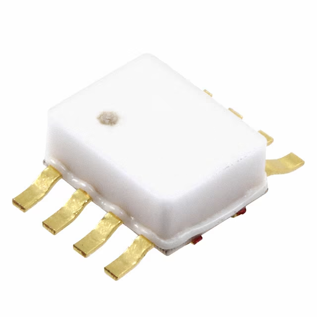
- Part No.:
- HMC347C8TR
- Manufacturer:
- Analog Devices Inc.
- Category:
- RF Switches
- Package:
- 8-CSOIC (0.154", 3.90mm Width) Exposed Pad
- Datasheet:
-
 HMC347C8TR.pdf
- Description:
- IC RF SWITCH SPDT 8GHZ 8CSMD
- Quantity:
- Payment:

- Shipping:

Inventory:3,791
Please send an inquiry. Send us your inquiry, and we will respond immediately.
Product details
Overview
HMC347C8TR from Analog Devices (formerly Hittite Microwave) is a GaAs MMIC SPDT switch in a non-hermetic surface-mount ceramic package, designed for RF signal routing in DC–8 GHz systems. It delivers >50 dB isolation up to 2 GHz, 2.0 dB typical insertion loss, and operates with -5/0 V complementary logic control without bias supply. It serves as a high-isolation replacement for HMC132C8 in microwave transceivers and test instrumentation.
For engineers reviewing the HMC347C8TR datasheet, HMC347C8TR pinout, HMC347C8TR application, or HMC347C8TR equivalent, key selection criteria include isolation vs. frequency, non-reflective architecture, thermal resistance (440 °C/W on insertion path), RF power handling (+27 dBm absolute max), and compatibility with 50 Ω RF layouts requiring grounded paddle soldering.
Technical Context
The HMC347C8TR implements a non-reflective GaAs MESFET topology with two independent RF paths (RFC→RF1 and RFC→RF2), controlled by complementary negative-voltage logic (CTLA/CTLB). Its design eliminates external bias networks and enables fast switching (tRISE/tFALL = 3 ns, tON/tOFF = 6 ns) across DC–8 GHz.
It features matched 50 Ω DC-coupled RF ports (RFC, RF1, RF2), requires PCB ground connection via all GND pins (2,3,8) and the exposed paddle, and mandates blocking capacitors when RF line DC potential ≠ 0 V. Thermal management relies on direct soldering of the copper-bottom package to RF ground plane.
Key Specifications
| Parameter | Value and Actual Design Meaning |
|---|---|
| Frequency Range | DC to 8 GHz - supports broadband RF routing from baseband through X-band without band switching. |
| Isolation | 54 dB max @ 2 GHz - ensures minimal crosstalk between RF1 and RF2 paths during state transition. |
| Insertion Loss | 2.0 dB typical @ DC–6 GHz - maintains signal integrity with low path attenuation in active configuration. |
| Input IP3 | 43 dBm typical @ 0.5–8 GHz - enables linear operation with two-tone +7 dBm inputs in receiver front-ends. |
| Switching Speed | tRISE/tFALL = 3 ns - supports high-speed TDD and pulse-modulated waveforms without timing skew. |
| Control Logic | -5 V / 0 V complementary - eliminates need for positive bias supply; compatible with standard negative logic drivers. |
| Thermal Resistance | 440 °C/W (insertion path) - defines junction-to-PCB thermal gradient under 19 dBm P1dB operation. |
Pinout & Package
Package: 8-lead non-hermetic ceramic SMT (white alumina body, copper bottom, electrolytic gold plating); dimensions per outline drawing - length/width exclude lid seal protrusion (0.005″/side); ground leads and paddle must be soldered to PCB RF ground.
| Pin/Terminal | Circuit Role | Design Meaning |
|---|---|---|
| 1, 4, 7 | RFC, RF1, RF2 | DC-coupled 50 Ω RF ports; require blocking capacitors if DC potential ≠ 0 V; RFC is common input, RF1/RF2 are selectable outputs. |
| 2, 3, 8 | GND | RF ground terminals; must be soldered to PCB ground plane; package bottom paddle is also GND and must be connected. |
| 5 | CTLA | Negative logic control input; "High" = 0 to -0.2 V, "Low" = -5 V ±0.5 V; selects RFC→RF1 path when High. |
| 6 | CTLB | Negative logic control input; "High" = 0 to -0.2 V, "Low" = -5 V ±0.5 V; selects RFC→RF2 path when High. |
Key Features
| Feature | Design Value |
|---|---|
| Non-reflective architecture | Terminates off-state ports internally to 50 Ω, preventing signal reflection and enabling stable VSWR in cascaded RF chains. |
| No external bias required | Operates solely from -5/0 V control lines - eliminates bias regulators, decoupling networks, and associated board area. |
| High ESD robustness | Class 1A (HBM) rating - withstands electrostatic discharge during handling and assembly without gate damage. |
| Thermally optimized package | Copper-bottom construction with soldered paddle achieves 440 °C/W thermal resistance - critical for +23 dBm P1dB operation. |
| DC-coupled RF ports | Enables baseband and modulated IF signal routing without AC coupling limitations or low-frequency roll-off. |
Applications
| 5G Massive MIMO Active Antenna Units | Microwave Point-to-Point Radios |
|---|---|
Use Scenario: Dynamic antenna calibration and T/R path selection in sub-6 GHz active arrays. IC Role / Device Role / Timing Role: SPDT switch routing calibration signals between transceiver IC and antenna elements. Use Value: >50 dB isolation at 2.5 GHz prevents calibration leakage into adjacent channels; 2.0 dB loss preserves SNR in feedback loops. |
Use Scenario: Dual-polarization diversity switching in 6–8 GHz backhaul radios. IC Role / Device Role / Timing Role: RF path selector enabling polarization agility without mechanical actuators. Use Value: 36 dB isolation at 8 GHz suppresses cross-polar interference; 3 ns rise time supports fast link reconfiguration. |
| Electronic Warfare ECM Front-Ends | Automated RF Test Systems |
Use Scenario: Fast-switching jammer signal injection into multi-band receiver chains. IC Role / Device Role / Timing Role: High-power RF switch isolating threat simulators from sensitive measurement receivers. Use Value: +27 dBm absolute max RF input withstands pulsed jammer outputs; non-reflective design avoids standing waves in wideband amplifiers. |
Use Scenario: Signal path multiplexing in vector network analyzer (VNA) calibration modules. IC Role / Device Role / Timing Role: Precision RF routing switch in automated calibration reference planes. Use Value: Stable 50 Ω match (13 dB return loss on-state) ensures traceable S-parameter accuracy; DC coupling supports low-frequency VNA sweeps. |
Equivalent & Alternatives
The following parts are listed as comparable options for similar SPDT switch applications.
| Alternative Part | Technical Difference | Application Difference | Selection Advice |
|---|---|---|---|
| HMC132C8TR | Lower isolation (45 dB @ 2 GHz), higher insertion loss (2.5 dB), same -5/0 V control and 8-lead ceramic package. | Less suitable for high-dynamic-range receivers where >50 dB isolation is required at L/S-band. | Choose HMC132C8TR only if cost sensitivity outweighs isolation and linearity requirements. |
| Qorvo QM11036 | Si-based, 0.1–6 GHz range, +3.3 V control, 2.2 dB loss, 42 dB isolation @ 2 GHz, different 6-pin DFN package. | Not suitable for DC-coupled or >6 GHz use; lacks non-reflective termination and ceramic thermal performance. | Consider QM11036 only for lower-frequency, low-cost, single-supply digital control environments. |
Compared with HMC132C8TR and QM11036, the HMC347C8TR provides superior isolation above 2 GHz, true DC–8 GHz bandwidth, and non-reflective operation - making it the only option among the three qualified for precision microwave test and military ECM systems requiring broadband, high-linearity, and thermally stable switching.
Availability
HMC347C8TR is available at Aetrix Electronics and suitable for telecom infrastructure, microwave radio & VSAT, and test instrumentation requiring stable component supply, full traceability, and long-term lifecycle support.
Supply support for HMC347C8TR includes scheduled delivery planning, volume procurement assistance, BOM continuity management, traceable sourcing, and lifecycle availability coordination for OEM customers, industrial embedded developers, connected-device designers, and electronics production programs.
Manufacturer
Analog Devices acquired Hittite Microwave in 2014 and integrates its high-frequency RF portfolio into ADI's broader signal chain solutions. The company specializes in precision analog, RF, and mixed-signal semiconductors.
The HMC347C8TR belongs to Hittite's legacy GaAs MMIC SPDT switch family, engineered specifically for high-isolation, broadband RF routing in defense, aerospace, and instrumentation applications where thermal stability and non-reflective behavior are critical.
FAQ
What is the maximum RF input power rating for the HMC347C8TR?
The HMC347C8TR has an absolute maximum RF input power rating of +27 dBm when control voltage is set to -5 V. However, caution is advised against "hot switching" above +13 dBm under standard -5/0 V control conditions. Derating is required above +23 dBm to maintain reliability, as confirmed by the 19–23 dBm P1dB range and 440 °C/W thermal resistance specification. Always refer to the absolute maximum ratings table in the official HMC347C8TR datasheet for safe operating limits.
Does the HMC347C8TR require external bias components?
No, the HMC347C8TR requires no external bias supply or passive components for basic operation. It functions using only complementary -5 V / 0 V control voltages applied to CTLA and CTLB pins. The internal GaAs MESFET architecture eliminates the need for bias resistors, decoupling capacitors, or level shifters - simplifying layout and reducing bill-of-materials cost compared to many competing SPDT switches.
How is the HMC347C8TR's non-reflective design implemented?
The HMC347C8TR implements non-reflective behavior by terminating the off-state RF port (e.g., RF2 when RFC→RF1 is active) into a matched 50 Ω load internally. This prevents signal reflections that would otherwise degrade VSWR and cause instability in cascaded stages. Measured return loss in the off-state reaches 9 dB at DC–2 GHz, confirming effective termination - a key advantage over reflective SPDT switches in sensitive receiver front-ends.
What is the recommended PCB grounding method for the HMC347C8TR?
The HMC347C8TR requires soldering all GND pins (2, 3, 8) and the exposed copper paddle on the package bottom directly to the PCB's RF ground plane. This dual-path grounding minimizes inductance and ensures optimal thermal dissipation (440 °C/W) and RF shielding. Failure to connect the paddle results in degraded isolation, increased insertion loss, and potential thermal runaway under high-power operation.
Can the HMC347C8TR be used in DC-coupled applications?
Yes, the HMC347C8TR supports true DC-coupled operation on all RF ports (RFC, RF1, RF2), enabling baseband and low-frequency IF signal routing. However, blocking capacitors must be added if the DC potential on any RF line differs from 0 V - as stated in the Pin Descriptions section. This capability distinguishes it from AC-coupled alternatives and makes it suitable for I/Q modulator/demodulator interfaces and calibration loopbacks.
HMC347C8TR Specifications
- Product attributes
- Attribute value
- Manufacturer:
- Analog Devices Inc.
- Series:
- -
- Package/Case:
- 8-CSOIC (0.154", 3.90mm Width) Exposed Pad
- Packaging:
- Tape & Reel (TR)
- Product Status:
- Obsolete
- RF Type:
- General Purpose
- Topology:
- -
- Circuit:
- SPDT
- Frequency Range:
- 0Hz ~ 8GHz
- Isolation:
- 40dB
- Insertion Loss:
- 2dB
- Test Frequency:
- 6GHz
- P1dB:
- 23dBm
- IIP3:
- 43dBm
- Features:
- -
- Impedance:
- 50Ohm
- Voltage - Supply:
- 5V
- Operating Temperature:
- -40°C ~ 85°C
- Grade:
- -
- Qualification:
- -
- Mounting Type:
- Surface Mount
- Supplier Device Package:
- 8-CSMD
HMC347C8TR FAQ
1.How can I place an order for HMC347C8TR through Aetrix?
Please submit a Request for Quotation (RFQ) for HMC347C8TR on Aetrix. Our sales agent will provide a competitive quotation and guide you through the order confirmation once you accept the terms.
2.Are the price and stock information for HMC347C8TR reliable?
The price and inventory of HMC347C8TR are updated periodically and may fluctuate due to market conditions. Stock and pricing data are typically refreshed every 24 hours. Quotation validity for HMC347C8TR is usually 5 days.
3.What payment methods are accepted for HMC347C8TR?
We accept Wire Transfer, PayPal, Credit Card, Western Union, MoneyGram, and Escrow for HMC347C8TR transactions.
Note: Certain payment methods may incur a processing fee.
4.How is shipping managed for HMC347C8TR?
HMC347C8TR orders can be shipped via leading logistics carriers, including DHL, UPS, FedEx, TNT, or Registered Mail.
Once your HMC347C8TR order is processed, you will receive an email with the shipment details and tracking number.
Note: Tracking information may take up to 24 hours to appear. Express delivery typically takes 3–5 business days.
5.How can I obtain technical support or documentation for HMC347C8TR?
For technical support, including HMC347C8TR datasheets, pinout diagrams, or application guidance, please contact our engineering support team. They can provide detailed documentation and assistance for your HMC347C8TR requirements.
6.How does Aetrix verify that HMC347C8TR is sourced from the original manufacturer or authorized distributors?
All HMC347C8TR products on Aetrix are procured from qualified distributors and authorized channels. Our dedicated quality assurance team conducts strict verification, including traceability checks and, if necessary, third-party testing. This ensures that HMC347C8TR meets industry standards.
7.What is the process for return or replacement of HMC347C8TR?
All HMC347C8TR units undergo pre-shipment inspection (PSI). If there is an issue with HMC347C8TR, returns or replacements are accepted under the following conditions:
1.Quantity discrepancies, incorrect items, or visible external defects (such as breakage or corrosion), acknowledged by Aetrix.
2.The issue is reported within 90 days of delivery.
3.The HMC347C8TR part is unused and in its original packaging.
Return procedure for HMC347C8TR:
1.Submit a request within 90 days.
2.Obtain a Return Material Authorization (RMA) from Aetrix.
HMC347C8TR Tags

-
BGS13SN8E6327XTSA1
Infineon Technologies
-
BGS12WN6E6327XTSA1
Infineon Technologies
-
BGS12P2L6E6327XTSA1
Infineon Technologies

-
BGS12PN10E6327XTSA1
Infineon Technologies
-
NJG1801K75-TE1
Nisshinbo Micro Devices Inc.
-
BGS14PN10E6327XTSA1
Infineon Technologies
-
SKY13348-374LF
Skyworks Solutions Inc.
-
4259-63
pSemi
-
PE42421SCAA-Z
pSemi
-
AS179-92LF
Skyworks Solutions Inc.
-
SKY13351-378LF
Skyworks Solutions Inc.
-
AS215-92LF
Skyworks Solutions Inc.
Tech Hub

A practical engineering guide to 3.3V and 5V logic compatibility, input thresholds, resistor dividers, translator ICs, MOSFET level shifting, I2C pull-ups, timing limits and power-sequencing risks.

The 74HC595 uses push-pull logic outputs, while the TPIC6B595 uses 50 V open-drain DMOS sinks for higher-power loads. This guide compares timing, current limits, 3.3 V interfacing, load wiring, thermal…

The 74HC595 converts serial data into eight stable parallel outputs. This guide covers pin functions, shift and storage timing, OE and MR behavior, drive-current limits, cascading, voltage compatibilit…

A technical comparison of level-sensitive latches and edge-triggered flip-flops, covering timing windows, setup and hold limits, master–slave operation, time borrowing, race-through, HDL inference and…

A D latch stores one bit while Enable controls when data can pass. This reference covers gate-level operation, truth tables, transparency, setup and hold timing, LE versus OE, common ICs and practical …

An SR latch stores one bit through cross-coupled feedback. This engineering reference covers NOR and NAND implementations, truth tables, forbidden-state recovery, gated operation, switch debouncing, fa…

Latch circuits retain one bit through feedback. This technical reference covers SR and D latches, truth tables, transparency, timing limits, latch-versus-flip-flop behavior, applications and common log…

An engineering guide to LED driver operation, constant-current and constant-voltage outputs, linear and switching topologies, dimming, IC selection, calculations, replacement compatibility, and fault c…

Operational amplifier guide covering op amp basics, feedback, ideal vs real op amps, common configurations, buffer circuits, offset, bias current, gain-bandwidth, slew rate, rail-to-rail limits and sel…

Jumper cables guide covering safe connection order, red and black clamp placement, final ground connection, cable gauge, length, clamp quality, copper vs CCA cables, jump starter comparison and battery…


