
 My Inquiry
 My Account


Analog Devices Inc. HMC7810ALC3
- Part No.:
- HMC7810ALC3
- Manufacturer:
- Analog Devices Inc.
- Category:
- Laser Drivers
- Package:
- 16-CLCC Exposed Pad
- Datasheet:
-
 HMC7810ALC3.pdf
- Description:
- IC LASER DRVR 32GBPS 3.3V 16LCC
- Quantity:
- Payment:

- Shipping:

Inventory:4,463
Please send an inquiry. Send us your inquiry, and we will respond immediately.
Product details
Overview
HMC7810ALC3 from Analog Devices is a differential-input/differential-output optical modulator driver IC with integrated analog attenuator and output peak detector, supporting up to 32.0 Gbps NRZ data rates, 28 GHz bandwidth, and 4.4 Vp-p differential output swing at 32 Gbps with VCTL = −1.5 V - designed for driving InP Mach-Zehnder or silicon photonics modulators in 400G/100G pluggable optical modules.
For engineers reviewing the HMC7810ALC3 datasheet, HMC7810ALC3 pinout, HMC7810ALC3 application, or HMC7810ALC3 equivalent, key selection considerations include its adjustable gain via VCTL (−1.5 V to 0 V), self-biased operation eliminating power sequencing, integrated VDET/VREF-based AGC interface, 16-terminal 2.9 mm × 2.9 mm LCC package, and compatibility with compact external bias tees for optical interconnect systems.
Technical Context
The HMC7810ALC3 implements a broadband linear amplifier architecture with fully differential signal path, no internal bias sequencing logic, and dual external supply rails (VDD = 3.3 V; VDD_EXTP/VDD_EXTN = 2.5 V or 3.3 V) enabling trade-offs between jitter (350 fs RMS at 2.5 V) and output swing (4.4 Vp-p at 3.3 V). Its analog attenuation control (VCTL) directly modulates small-signal gain from 4 dB to 18 dB over 1 MHz–28 GHz.
Integrated peak detection uses VDET and VREF outputs to generate VPEAK = VDET − VREF, a voltage linearly proportional to differential output swing (e.g., 4.5 Vp-p → ~3.0 V VPEAK), enabling closed-loop automatic gain control without external RF detectors. Input and output impedances are matched to 100 Ω differential / 50 Ω single-ended, with return loss ≥10 dB across 1–30 GHz depending on VCTL setting.
Key Specifications
| Parameter | Value and Actual Design Meaning |
|---|---|
| Max Data Rate | 32.0 Gbps NRZ (PRBS31), enabling 400G 16-QAM and 100G DP-QPSK optical module support |
| Bandwidth | 28 GHz high-frequency cutoff, 1 MHz low cutoff - supports full C-band optical modulation |
| Differential Output Swing | 4.4 Vp-p at 32 Gbps with VCTL = −1.5 V, sufficient to drive InP MZ modulators requiring >3.5 Vp-p |
| Rise/Fall Time | 13 ps (20%–80%), ensuring clean eye opening and low deterministic jitter (≤3 ps) |
| Gain Adjustment Range | 4 dB to 18 dB differential-to-differential gain via analog VCTL (−1.5 V to 0 V), enabling dynamic linearity optimization |
| Power Consumption | 0.5 W at 3.3 V external supplies; 0.44 W at 2.5 V - scalable for thermal-constrained optical modules |
| Output Jitter (RMS) | 350 fs at 2.5 V supplies, critical for maintaining BER <10−12 in coherent systems |
Pinout & Package
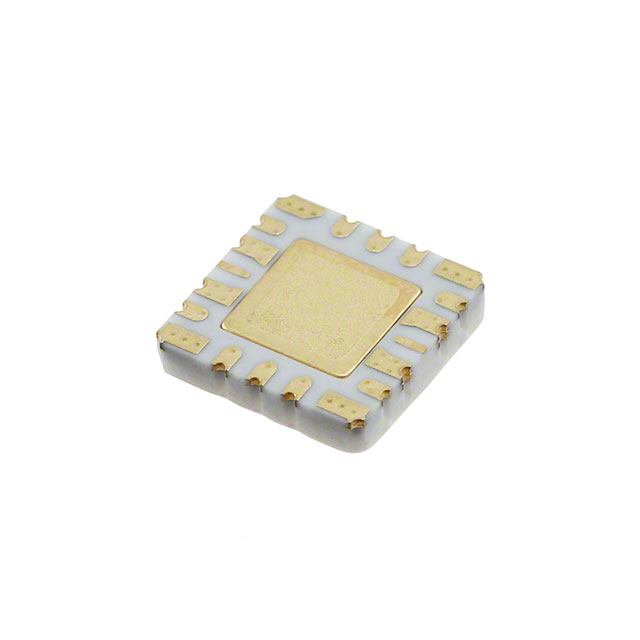
Package: 16-terminal, 2.9 mm × 2.9 mm leadless chip carrier (LCC), exposed thermal pad (EPAD) requiring connection to GND per JEDEC E-16-1 standard.
| Pin/Terminal | Circuit Role | Design Meaning |
|---|---|---|
| 1, 4, 9, 12 | GND | Supply ground connections; EPAD must be soldered to PCB GND plane for thermal and electrical integrity |
| 2 | INN | Negative differential input; AC-coupled, 100 Ω differential impedance |
| 3 | INP | Positive differential input; AC-coupled, 100 Ω differential impedance |
| 5, 7, 14 | NIC | Not internally connected - must remain unconnected or grounded per layout guidelines |
| 6 | VCTL | Analog attenuator control voltage input (−1.5 V to 0 V); sets gain and output swing |
| 8 | VC | Amplitude control voltage input (0–1.5 V); fine-tunes output level independent of VCTL |
| 10 | OUTP | Positive differential output; requires external bias tee for DC restoration to modulator |
| 11 | OUTN | Negative differential output; requires external bias tee for DC restoration to modulator |
| 13 | VREF | Reference voltage for integrated peak detector; used with VDET to compute VPEAK |
| 15 | VDET | Detector output voltage; VPEAK = VDET − VREF provides linear measure of output swing |
| 16 | VDD | Main supply (3.3 V); powers core amplifier and control circuitry |
Key Features
| Feature | Design Value |
|---|---|
| Self-biased architecture | Eliminates power supply sequencing requirements - simplifies system startup and reduces BOM count |
| Integrated peak detector (VDET/VREF) | Enables real-time, analog closed-loop AGC without external RF detectors or ADCs |
| Adjustable gain via VCTL | 6 dB+ gain range (4–18 dB) with flatness ±1 dB from 1–20 GHz supports adaptive linearity tuning |
| Dual external supply options | VDD_EXTP/VDD_EXTN selectable at 2.5 V (low jitter) or 3.3 V (high swing) - runtime-configurable trade-off |
| Compact LCC package | 2.9 mm × 2.9 mm footprint with exposed pad enables high-density optical module layouts |
Applications
| 400G CFP2 Optical Transceiver | 100G DP-QPSK Metro Module |
|---|---|
|
Use Scenario: Driving dual-polarization quadrature phase-shift keying (DP-QPSK) Mach-Zehnder modulators in CFP2 pluggable transceivers for metro DWDM networks. IC Role / Device Role / Timing Role: High-linearity broadband driver providing 32 Gbps differential signals with sub-3 ps deterministic jitter and 4.4 Vp-p swing to maintain extinction ratio >12 dB. Use Value: Integrated VDET/VREF enables automatic output swing calibration during temperature drift, reducing need for field recalibration and improving long-term BER stability. |
Use Scenario: Biasing electroabsorption modulated laser (EML) transmitters in short-reach 100G-LR4 modules using single-ended output configuration. IC Role / Device Role / Timing Role: Differential-to-single-ended gain stage delivering 2.2 Vp-p output with 13 ps rise/fall time to meet IEEE 802.3ba 100GBASE-LR4 eye mask requirements. Use Value: Self-biased operation eliminates sequenced power supplies, reducing PCB area and cost in space-constrained SFP28 form factors. |
| Broadband Test Equipment | Silicon Photonics Co-Packaged Optics |
|
Use Scenario: Signal source in high-speed bit-error-rate testers (BERTs) and vector network analyzers requiring stable, wideband RF amplification up to 30 GHz. IC Role / Device Role / Timing Role: Gain-flat broadband amplifier with ±1 dB flatness from 1–20 GHz and group delay variation ±7.5 ps, enabling accurate frequency-domain characterization. Use Value: External VCTL control allows real-time gain adjustment during sweep measurements without hardware reconfiguration. |
Use Scenario: Modulator driver in co-packaged optics (CPO) architectures where silicon photonics chips require tightly controlled, low-jitter drive signals adjacent to ASICs. IC Role / Device Role / Timing Role: Low-power (0.44 W at 2.5 V) driver with 350 fs RMS jitter minimizing timing uncertainty in high-channel-count parallel optical links. Use Value: Exposed thermal pad and 51 °C/W θJC enable direct thermal coupling to CPO substrate, maintaining junction temperature <105°C under continuous 32 Gbps operation. |
Equivalent & Alternatives
The following parts are listed as comparable options for similar optical modulator driver applications.
| Alternative Part | Technical Difference | Application Difference | Selection Advice |
|---|---|---|---|
| HMC981LP3E | Higher 40 Gbps max rate but no integrated peak detector or VCTL-based gain control; requires external AGC loop | Targeted at ultra-high-speed test equipment rather than production optical modules with closed-loop calibration needs | Select when maximum bandwidth (>30 GHz) outweighs need for on-chip AGC functionality |
| LMH5401RTVT | Lower 18 GHz bandwidth, 2.5 V supply only, no VCTL pin - fixed-gain architecture with integrated bias tee | Designed for lower-cost 25G/50G SR applications, not 100G/400G coherent or DP-QPSK systems | Select for cost-sensitive, lower-data-rate EML drivers where board space permits external bias tee integration |
Compared with HMC7810ALC3, HMC981LP3E offers higher bandwidth but lacks integrated AGC capability, increasing system complexity; LMH5401RTVT reduces component count via integrated bias tee but sacrifices both bandwidth and programmable gain - making HMC7810ALC3 the optimal choice for production 100G/400G modules requiring calibrated, adaptive drive performance.
Availability
HMC7810ALC3 is available at Aetrix Electronics and suitable for 400G CFP2 transceivers, 100G DP-QPSK metro modules, and broadband test instrumentation requiring stable component supply, RoHS compliance, and guaranteed long-term availability through 2030.
Supply support for HMC7810ALC3 includes scheduled delivery planning, volume procurement assistance, BOM continuity management, traceable sourcing, and lifecycle availability coordination for OEM customers, industrial embedded developers, connected-device designers, and electronics production programs.
Manufacturer
Analog Devices is a global leader in high-performance analog, mixed-signal, and RF ICs, serving precision instrumentation, communications, and industrial markets since 1965.
The HMC7810ALC3 belongs to Analog Devices' Hittite Microwave product line, engineered specifically for high-speed optical interconnect applications demanding low jitter, wide bandwidth, and integrated control features in compact packages.
FAQ
What is the maximum data rate supported by the HMC7810ALC3?
The HMC7810ALC3 supports a maximum data rate of 32.0 Gbps using nonreturn-to-zero (NRZ) encoding with a pseudorandom binary sequence (PRBS31). This specification is validated under typical conditions at 25°C with VDD = 3.3 V and VDD_EXTP/VDD_EXTN = 2.5 V or 3.3 V. The HMC7810ALC3 maintains signal integrity at this rate with 13 ps rise/fall times and ≤3 ps deterministic jitter, making it suitable for 400G and 100G optical standards.
Does the HMC7810ALC3 require external power supply sequencing?
No, the HMC7810ALC3 is self-biased and does not require power supply sequencing. It operates reliably with simultaneous application of VDD = 3.3 V and VDD_EXTP/VDD_EXTN = 2.5 V or 3.3 V. This eliminates the need for complex power management ICs or timing controllers in optical module designs, simplifying system architecture and improving startup robustness - a key advantage confirmed in the HMC7810ALC3 datasheet Rev. A, Page 10.
How is automatic gain control implemented using the HMC7810ALC3?
Automatic gain control (AGC) is implemented using the HMC7810ALC3's integrated peak detector: VPEAK = VDET − VREF provides a DC voltage linearly proportional to the differential output swing. This voltage is fed into an external analog or digital controller that adjusts the VCTL pin (−1.5 V to 0 V) to maintain constant output amplitude. The HMC7810ALC3 datasheet Figure 17 shows a complete AGC loop schematic, confirming this method enables real-time compensation for temperature and aging effects without external RF detectors.
What package type and thermal characteristics does the HMC7810ALC3 use?
The HMC7810ALC3 uses a 16-terminal leadless ceramic chip carrier (LCC) package, 2.9 mm × 2.9 mm, with an exposed thermal pad (EPAD) that must be soldered to PCB ground. Its thermal resistance is θJA = 53 °C/W and θJC = 51 °C/W (JEDEC 2S2P board), enabling operation from −40°C to +130°C ambient. The exposed pad is essential for meeting the 175°C maximum junction temperature limit under full 0.5 W power dissipation - specified in the HMC7810ALC3 datasheet Absolute Maximum Ratings table.
Can the HMC7810ALC3 drive both InP Mach-Zehnder and silicon photonics modulators?
Yes, the HMC7810ALC3 is explicitly qualified to drive both indium phosphide (InP) Mach-Zehnder modulators and silicon photonics modulators, as stated in the General Description (Page 1) and Applications (Page 1) sections of the HMC7810ALC3 datasheet. Its 4.4 Vp-p differential output swing, 28 GHz bandwidth, and low THD (<3% at 4 Vp-p) meet the stringent linearity and drive strength requirements of both technologies in data center interconnect and co-packaged optics applications.
HMC7810ALC3 Specifications
- Product attributes
- Attribute value
- Manufacturer:
- Analog Devices Inc.
- Series:
- -
- Package/Case:
- 16-CLCC Exposed Pad
- Packaging:
- Bulk
- Product Status:
- Obsolete
- Type:
- Laser Diode Driver
- Data Rate:
- 32Gbps
- Number of Channels:
- 1
- Voltage - Supply:
- 3.3V
- Current - Supply:
- -
- Current - Modulation:
- -
- Current - Bias:
- -
- Operating Temperature:
- -40°C ~ 130°C
- Grade:
- -
- Qualification:
- -
- Supplier Device Package:
- 16-LCC (2.9x2.9)
- Mounting Type:
- Surface Mount
HMC7810ALC3 FAQ
1.How can I place an order for HMC7810ALC3 through Aetrix?
Please submit a Request for Quotation (RFQ) for HMC7810ALC3 on Aetrix. Our sales agent will provide a competitive quotation and guide you through the order confirmation once you accept the terms.
2.Are the price and stock information for HMC7810ALC3 reliable?
The price and inventory of HMC7810ALC3 are updated periodically and may fluctuate due to market conditions. Stock and pricing data are typically refreshed every 24 hours. Quotation validity for HMC7810ALC3 is usually 5 days.
3.What payment methods are accepted for HMC7810ALC3?
We accept Wire Transfer, PayPal, Credit Card, Western Union, MoneyGram, and Escrow for HMC7810ALC3 transactions.
Note: Certain payment methods may incur a processing fee.
4.How is shipping managed for HMC7810ALC3?
HMC7810ALC3 orders can be shipped via leading logistics carriers, including DHL, UPS, FedEx, TNT, or Registered Mail.
Once your HMC7810ALC3 order is processed, you will receive an email with the shipment details and tracking number.
Note: Tracking information may take up to 24 hours to appear. Express delivery typically takes 3–5 business days.
5.How can I obtain technical support or documentation for HMC7810ALC3?
For technical support, including HMC7810ALC3 datasheets, pinout diagrams, or application guidance, please contact our engineering support team. They can provide detailed documentation and assistance for your HMC7810ALC3 requirements.
6.How does Aetrix verify that HMC7810ALC3 is sourced from the original manufacturer or authorized distributors?
All HMC7810ALC3 products on Aetrix are procured from qualified distributors and authorized channels. Our dedicated quality assurance team conducts strict verification, including traceability checks and, if necessary, third-party testing. This ensures that HMC7810ALC3 meets industry standards.
7.What is the process for return or replacement of HMC7810ALC3?
All HMC7810ALC3 units undergo pre-shipment inspection (PSI). If there is an issue with HMC7810ALC3, returns or replacements are accepted under the following conditions:
1.Quantity discrepancies, incorrect items, or visible external defects (such as breakage or corrosion), acknowledged by Aetrix.
2.The issue is reported within 90 days of delivery.
3.The HMC7810ALC3 part is unused and in its original packaging.
Return procedure for HMC7810ALC3:
1.Submit a request within 90 days.
2.Obtain a Return Material Authorization (RMA) from Aetrix.
HMC7810ALC3 Tags
-
EPC21701
EPC
-
EPC21601
EPC
-
MAX3799ETJ+T
Analog Devices Inc./Maxim Integrated
-
AD9665ACPZ-REEL7
Analog Devices Inc.

-
MAX3740AETG+T
Analog Devices Inc./Maxim Integrated
-
MAX3795ETG+
Analog Devices Inc./Maxim Integrated

-
EPC21603
EPC
-
ONET8501VRGPT
Texas Instruments
-
MAX3738ETG+T
Analog Devices Inc./Maxim Integrated
-
SY88022ALMG-TR
Microchip Technology
-
ISL78365ARZ-T7A
Renesas
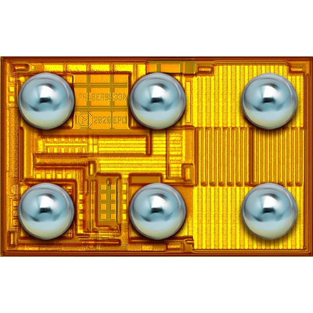
-
EPC21603ENGRT
EPC
Tech Hub

A practical engineering guide to 3.3V and 5V logic compatibility, input thresholds, resistor dividers, translator ICs, MOSFET level shifting, I2C pull-ups, timing limits and power-sequencing risks.

The 74HC595 uses push-pull logic outputs, while the TPIC6B595 uses 50 V open-drain DMOS sinks for higher-power loads. This guide compares timing, current limits, 3.3 V interfacing, load wiring, thermal…

The 74HC595 converts serial data into eight stable parallel outputs. This guide covers pin functions, shift and storage timing, OE and MR behavior, drive-current limits, cascading, voltage compatibilit…

A technical comparison of level-sensitive latches and edge-triggered flip-flops, covering timing windows, setup and hold limits, master–slave operation, time borrowing, race-through, HDL inference and…

A D latch stores one bit while Enable controls when data can pass. This reference covers gate-level operation, truth tables, transparency, setup and hold timing, LE versus OE, common ICs and practical …

An SR latch stores one bit through cross-coupled feedback. This engineering reference covers NOR and NAND implementations, truth tables, forbidden-state recovery, gated operation, switch debouncing, fa…

Latch circuits retain one bit through feedback. This technical reference covers SR and D latches, truth tables, transparency, timing limits, latch-versus-flip-flop behavior, applications and common log…

An engineering guide to LED driver operation, constant-current and constant-voltage outputs, linear and switching topologies, dimming, IC selection, calculations, replacement compatibility, and fault c…

Operational amplifier guide covering op amp basics, feedback, ideal vs real op amps, common configurations, buffer circuits, offset, bias current, gain-bandwidth, slew rate, rail-to-rail limits and sel…

Jumper cables guide covering safe connection order, red and black clamp placement, final ground connection, cable gauge, length, clamp quality, copper vs CCA cables, jump starter comparison and battery…


